In this paper, the nominal fitting accuracy and some dynamic ranges of the four active filter design tools are evaluated in detail. All four tools use an ideal op amp with a nominal fitting error of less than 0.6% and an E96 step resistor value, which is excellent in terms of nominal fitting accuracy. Operating with a minimum gain-bandwidth amplifier can save a considerable amount of power, but it should be combined with the GBW adjustment method to reduce the nominal fitting error.
What are the benefits of using a multi-feedback (MFB) low-pass active filter tool from a supplier? Let's dig deeper to get the answer.
In the exploration of the accuracy of this online design tool, the four suppliers' tools available on the market for RC values ​​given by relatively simple second-order low-pass filters are implemented in the MFB topology. This article will use these values ​​for simulation to compare the resulting filter shape with the ideal target to find the fit error for each solution. The nominal fit error is caused by the standard value of the RC constraint and the gain bandwidth product (GBW or GBP) of the finite amplifier. The output point and integrated noise results for each RC scheme obtained using the same op amp model are slightly different due to the difference in resistance magnitude and peak noise gain.
The noise gain shape in the MFB filter results from the desired filter shape and noise gain zeros. Because the noise gain zeros given by a particular RC scheme are different, the peak noise gains of different schemes are very different. The design example will explain these differences and also show the difference of the minimum in-loop gain (LG) of the RC scheme for different tools.
First, the nominal gain response and the ideal response of the fitting errorThere are many ways to evaluate the fitting error. All these tools have very similar response shapes in most frequency ranges, with most of the deviations occurring near the peak of the response. A simple measure of fit is to compare each of the f0 and Q derived from the implementation circuit with its ideal target and derive their percentage error. Then find the root mean square (RMS) of these two errors to get a combined error indicator.
Regardless of the op amp design choice, ADI tools allow the download of simulation data - here is the LTC6240. To continue to compare the noise and loop gains of different schemes, the RC scheme was migrated to TINA, while LMP7711 was used as the common op amp for noise simulation of each scheme. Since the ADI tool is also used for a slightly different filter shape (1.04dB peak vs. 1.0dB in other tools), for comparison, it first isolates its response fitting results.
ADI target response shape:
Av = -10V/V (20dB) fpeak = 54.34kHz f-3dB = 100kHz Q = 0.9636 (1.04dB peak) fo = 80kHz
Using the circuit in Figure 1 (and the RC number shown), these two ADI solutions will be simulated using the LTC6240 in the ADI tool and the LMP7711 in TINA (Figure 1 uses the TINA setting of the LMP7711). The key requirement to achieve an effective fit comparison is the true single-pole open-loop gain bandwidth product of the op amp. Using the TINA model to test the LMP7711 Aol (Open Loop Gain) response shows a 26 MHz GBW result, while its reported value is 17 MHz GBW. Prior to the simulation, the model was modified to 17 MHz (C2 increased from 20 pF to 33.3 pF in the macro) so that the results obtained can be compared with the LTC6240 simulation data obtained from the ADI tool. For ease of Aol testing, the LTC6240 does not appear in the TINA library, but we assume it meets the data sheet's GBW = 18MHz.
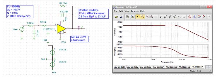
Figure 1: The ADI's uncorrected RCW of the GBW is given in TINA and the LMP7711 active filter simulation is used.
The first level that does not match the target is the standard resistance value selection. There are 5 RC values ​​to choose from, but there are only 3 design goals. Usually the E24 (5% step size) capacitance value is selected first, and then the final result of the exact resistance of E96 (1% step size) is obtained for 3 design goals. These values ​​can be placed in an ideal (infinite GBW) formula to first estimate how much error this step is expected to have. Selecting the standard capacitor value first, the standard value of the three resistor precision schemes will be higher and lower than the exact result. Although it is unlikely to be implemented in these current tools, in the future, a fitting proximity test can be performed on the eight standard values ​​above or below the exact value, and then “turned†from the exact value to the standard value with the least error. The more common situation is that the three accurate value resistors use the closest standard value. Based on the proximity of the exact value to the standard E96 resistance value, the fitting error has a certain degree of randomness.
These values ​​can then be applied to a finite GBW op amp model and simulated before the RC tolerance is applied to arrive at the final nominal fitting error. Table 1 summarizes the data downloaded from the ADI tool using the LTC6240 model and the data downloaded from TINA using the modified GBW LMP7711 model. Note that using these nominal standard RC values, no single GBW op amp simulation can achieve the desired 100 kHz f-3 dB frequency within 1%.
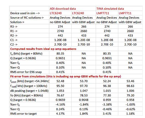
Table 1: List of fitting error results for ADI targets and scenarios.
The ideal op amp value assumes an infinite GBW, which is caused only by the selected standard resistance value. The GBW-adjusted RC value cannot be applied to the ideal formula because its goal seems wrong. Using the actual op amp model to display the nominal results, RC values ​​were not adjusted for GBW, resulting in a large root mean square error of 3.4% to 4.2%. This is because this design chose an ultra-low GBW device. The ADI GBW-adjusted RC value greatly improves this situation, so that the nominal root-mean-square error of fo and Q is only 1.2% to 1.8%. As expected, they are slightly higher than the 0.41% error of selecting the E96 standard resistance value. Figure 2 compares these simulation results with ideal values ​​and zooms in near the peak.
These nominal response shapes are close to but not exactly in line with the target. The effect of RC device tolerances further expands the expected response shape that has shifted the nominal result. The grey LMP7711 RC values ​​are governed by GBW and appear to be the worst-fit in the graph, with the worst fit to Q, but have the least RMS fitting error and are fitted with fo and the resulting f-3dB the best. Obviously, if the nominal response has drifted relative to the target, then there is still a long way to go to improve this fit to provide more target-centric expansion when including RC tolerances (Note: ADI Tools Responsive extended envelope data download is also provided - but this is beyond the scope of this article.)
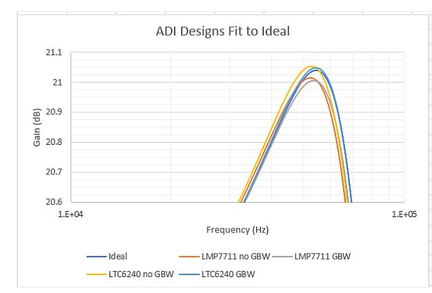
Figure 2: Close-up of the response match around the 1.04 dB target peak at 54.34 kHz.
Continue to use RC results from TI and Intersil tools. Here are some slightly different goals:
Av = -10V/V (20dB) fpeak = 54.08kHz f-3dB = 100kHz Q = 0.957 (1.0dB peak) fo = 80.26kHz fcutoff or fpassband = 76.49kHz
All of these tools seem to only provide RC solutions for "ideal" op amps. To test the effect of using a relatively slow device (17MHz, LMP7711), only the RC values ​​of Webench and Intersil are used here, and the results of simulations using the 150MHz GBW OPA300 model are also shown.
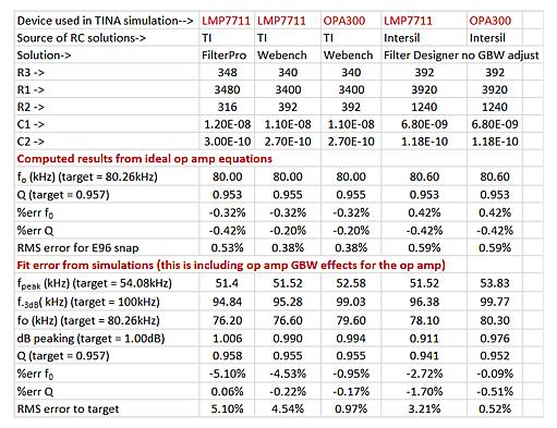
Table 2: Summary of Design and Target Fit Errors for TI and Intersil Solutions.
For the ideal op amp equation, the initial error of the relative standard resistance appears to be in the range of 0.38% to 0.59%. Assuming there is an ideal op amp, downloading the first and second columns of response data from Filterpro shows a similar initial error. When using the 17MHz GBW (LMP7711) model for simulation, the error increased from 3.21% to 5.1%. Using a more "ideal" device (such as 150MHz GBW OPA300) to rerun, the error is reduced to less than 1% RMS. Figure 3 shows the response shape of the Table 2 design near the peak gain.
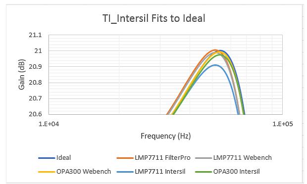
Figure 3: Close-up of response match amplification near the 1.0 dB target peak at 54.08 kHz.
The best fit here is the RC value from Intersil (assuming it is a perfect op amp) and the much faster OPA300. It appears that using the device at the low end of the GBW recommended by the ADI tool results in a relatively large nominal fitting error. Where it is necessary to use lower GBW (and power) devices, it is prudent to use an RC program that adjusts the GBW. Obviously, using a much faster device like the OPA300 can improve the fitting accuracy - but in these examples, the price is that the OPA300's current is as high as 12mA, while the LMP7711 is only 1.15mA.
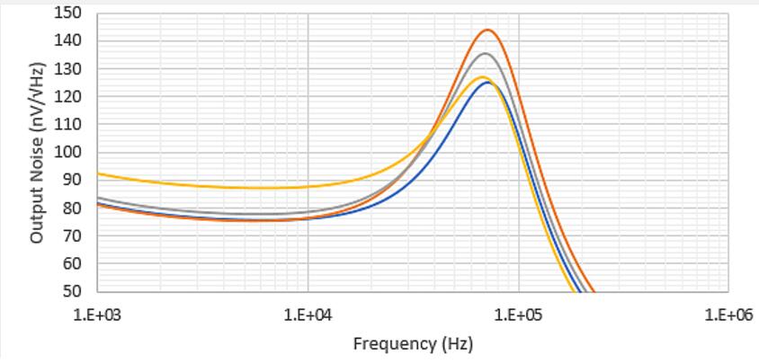
Second, the output point noise and SNR of different schemesAssuming that the inherent input voltage noise of the LMP7711, LTC6240, and ISL28110 op amps is approximately 6nV to 7nV, adjust the filter's RC scheme. For simplicity, noise comparisons will be done in TINA using the LMP7711 model. Examining this model, the input noise in the flat band is 4.9 nV/√Hz rather than the 5.9 nV at a higher frequency than the 1/f rotation angle given in the data sheet. In order to increase the apparent input voltage noise of these simulations to approximately 6.0nV as assumed in the RC scheme, it is only necessary to add a 602Ω resistor ground to the non-inverting input before performing the MFB noise comparison simulation and then use the op amp model noise to perform Root mean square processing. Since this is a CMOS input amplifier, it is safe to ignore the effects of input current noise. Figure 4 shows the circuit and output point noise of a GBW-adjusted RC value generated using the ADI tool. A new component in the simulation is a grounded 602Ω resistor added to the noninverting input to generate op amp model data when combined with the inherent 4.9nV/√Hz derived from a simple 100V/V test simulation gain. 5.9 nV/√Hz data specified in the manual.
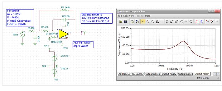
Figure 4: Example of output point noise using the LMP7711 model, RC scheme adjusted by ADI tool.
The point noise curve of FIG. 4 shows a 1/f corner at the 1 kHz start point, then flattens in the middle frequency region and peaks near the resonance frequency. Due to the noise gain peak (NG) inherent in this topology, most active filter designs show this noise spike. Four design examples will use this simulation to derive flatband and peak noise.
One way to look at the integral noise is to make the SNR form a specific expected maximum Vpp output. These design examples are also simulated for SNR and integrated to 1 MHz using the 4Vpp maximum output assumption (entering 1.414Vrms 4Vpp RMS value in the noise panel of TINA). Table 3 summarizes the noise simulation results using four designs.
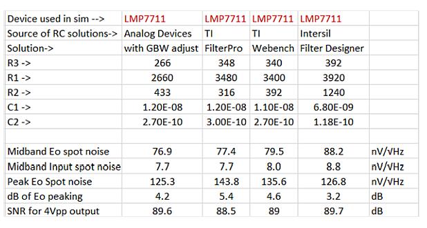
Table 3: Noise simulation results.
Figure 5 is a plot of output point noise versus frequency using the LMP7711 TINA model to simulate the four sets of RC values ​​in Table 3.
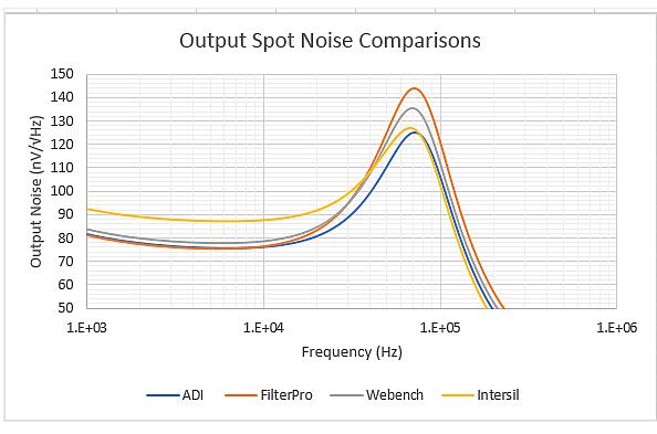
Figure 5: Output point noise simulation comparison.
Observe the noise plot in Figure 5 and get the following conclusion:
The Intersil value gives the highest flatband noise (highest resistance) but the lowest peak at this level;
The flat band noise of the other three designs is almost the same, where the ADI design has the smallest peak;
The Peak of the FilterPro design is highest because the input resistance is greater than the resistance within the loop;
The input reference noise in the flatband is not much larger than the 5.9nV/Hz of the LMP7711 model +602Ω noise. This shows that the resistance has been adjusted to only slightly affect the overall result. The difference in the R2/R3 ratio (and resulting noise gain zero position) has a greater effect on the integrated noise and the corresponding SNR;
The signal-to-noise ratio of the ADI and Intersil RC solutions is better than that of the FilterPro design by more than 1 dB. This is because FilterPro's designed noise gain zeros are wider than those of the other three solutions. These differences are due to the fact that the RC schemes all target the same filter response shape.
Third, the noise gain (NG) peak and loop gain (LG) analysisThe inherent noise gain of the MFB topology frequency response peaks with frequency changes. The peaks are due to the desired frequency response poles and noise gain zeros - they are controlled to produce more or less in-band peaks while still providing the desired shape of the closed-loop response. The MFB noise gain of the circuit of Figure 1 is given by Equation 1, and the numerator of the equation (used to solve the transfer function zero) is written as much as possible based on the target response shape.
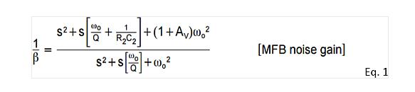
In addition to the 1/(R2C2) integral in the inner ring, the molecule is completely constrained by the desired filter pole. This shows that you can use the integral link ratio to move the zero within a certain limit. The zero point of the MFB noise gain is always a real number, but it can be described by the familiar ωz and Qz formats similar to the denominator in Equation 1. Qz is always "0.5", indicating that there are 2 real zeros. To obtain ωz and Qz and zero, solve the numerator of Equation 1, and get Equations 2 and 3, which are written according to the desired active filter poles ω0 and Qp.
The zero point falls above and below the desired filter f0, and increasing Qz to 0.5 will increase the zero frequency below. This can reduce the peak noise gain with frequency and increase the passband LG for any selected op amp.
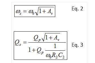
Each of the schemes in Table 3 can use Equation 1 to analyze the NG shape, use Equation 3 to derive Qz, and solve the lower noise gain zeros. Then use Equation 1 to generate different NG versus frequency curves for different RC schemes in Table 3, as shown in Figure 6. This shows that all schemes for the same closed-loop response have large differences in peak NG.
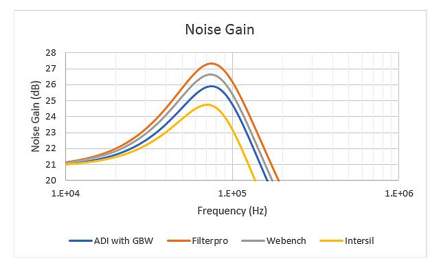
Figure 6: Noise gain response shape for different RC schemes in Table 3.
Combining the NG curve with the Aol curve of the LMP7711 and generating the difference as LG yields the minimum loop gain. The example in Figure 7 calculates the noise gain of the Intersil RC scheme in Table 3, showing the 17MHz Aol curve of the LMP7711, and the corresponding LG.
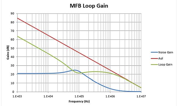
Figure 7: Noise Gain and resulting loop gain for Intersil RC values ​​in Table 3 and LMP7711 Aol.
All second-order low-pass MFB LG plots exhibit similar characteristics to those of FIG. 6 . Key points include:
The AOL curve of the LMP7711 uses 17 MHz GBW. From the 40dB gain line, it passes through 170kHz and is multiplied by 100 times;
The NG curve shows the peak characteristics near f0. In this case, for the design example using the Intersil RC value in Table 3, the peak value is reduced (as shown in Figure 6);
For the desired filter shape, when NG falls above f-3dB, LG reaches a minimum near the maximum noise gain, and remains relatively flat over a range of frequencies from here to about 10 times f-3dB;
NG is close to 0dB (1V/V) at higher frequencies due to the feedback capacitor in the design. This shows that a unity-gain-stabilized op amp is needed. The solution to this constraint is to use an extra ground capacitor at the inverting input. In the FDA-based MFB filter design, to improve loop phase margin, a differential capacitor can be connected across the input when needed to create a higher noise gain at the intersection of LG = 0dB.
The minimum LG and filter response shape around f0 influence each other in several ways:
Because the loop gain is lowest, this will be the peak gain error frequency in the response;
This will also be the maximum closed-loop output impedance over the entire response range;
The minimum loop gain also means minimum harmonic distortion suppression.
Gain bandwidth adjustment routines typically include op amp Aol effects, but seldom include output impedance peaks. LG reduces the open-loop output impedance of a particular device, but the open-loop output impedance may be very reactive in itself, until recently well-modeled in modern rail-to-rail output devices.
Table 4 summarizes the noise gain Qz, the resulting lower noise gain zero, the NG peak, and the minimum loop gain for the four program examples given by the four different tools. The reported peak noise gain is an increase in the DC value of 20*log(11V/V)=20.8dB. The 11V/V DC noise gain is assumed to be driven by a zero-ohm power supply.
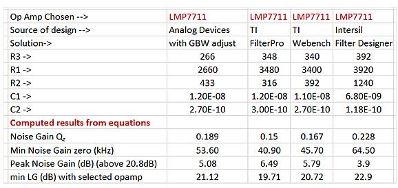
Table 4: Summary of NG Qz and lower NG zero frequency with NG peak and LG minima.
Where possible, it is better to pull the lower noise gain zero within the other constraints to make it as close to f0 as possible. The IntersilRC solution has already done so, where the peak value from the DC noise gain (20.8dB, 11V/V) is reduced - about 2.6dB lower than the Filterpro solution. Note that the peak NG in all four solutions is significantly higher than the 1 dB target peak in the response shape. The lower noise gain zero controls this maximum NG peak, and it has the greatest effect on the minimum loop gain value and SNR in a lowpass active filter design that is not too large for this peak. The minimum loop gain for all four designs is relatively low, which is due to the selected 17MHz GBW device. There are several reasons to use higher GBW devices (above the 17 MHz selected here):
The nominal deviation of the response shape is lower than the desired target;
The smallest LG in the f0 region is higher;
Lower output harmonic distortion;
The lower closed-loop output impedance—interacts with the accuracy of the response shape and the ability to accurately drive the load.
Starting with the minimum GBW design here, using a faster op amp directly affects the smallest LG. For example, using 150MHz OPA300 and 17MHz LMP7711 will increase the minimum LG in Table 4 by 20log(150/17) = 18.9dB. Applications that face the time domain are generally more tolerant of lower minimum LGs. Where the lowest harmonic distortion is needed, consider using devices that are faster and have the smallest increase in quiescent current.
Table 5 summarizes the performance of the four design examples using the modified LMP7711 model. Obviously, small differences in the RC scheme can result in significantly different final nominal performance.
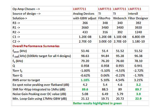
Table 5: Summary of LMP7711 op amp selection results.
IV . Summary of Comments and SuggestionsThis article evaluates in detail the nominal fitting accuracy and some dynamic ranges. All 4 tools use ideal op amps and have achieved good nominal fitting accuracy - when choosing the E96 step resistance value, the nominal fitting error is 0.6%. All response shapes deviate from the goal, including a true op amp - so no perfect nominal fit to the goal should be expected. Operating with a minimum gain-bandwidth amplifier can significantly save power, but it should be used in conjunction with the GBW adjustment method to reduce the nominal fitting error.
Newer tools (ADI, Webench, and Intersil) can adjust R values ​​to fit the op amp's inherent input noise specifications. However, the main mechanism for distinguishing integral noise is the layout of noise gain zeros. Intersil tools can increase Qz and reduce noise gain peaks. It is unclear how the other three tools treat this strategy.
Tool development and design suggestions:
1, taking into account the indicators mentioned in this article, when selecting the amplifier, pay attention to balance GBW margin and power consumption;
2. Validate the op amp model before testing as much as possible, and make corresponding changes when needed to improve the effectiveness of the results;
3. Use GBW adjustment algorithms to extend the applicable space of the solution to much lower speed/power op amps and/or to increase the accuracy of nominal fitting;
4. The RC solution is biased towards higher noise gain Qz, which will increase SNR and improve LG in the NG peak region;
5. For each second level, allow the target pole to be set directly. In this way, designs generated with some of the more powerful third-party tools can be implemented in the op amp vendor tool to better bind the RC solution to the op amp parameters;
6. Leave a 2% capacitance tolerance in the 5% E24 step size and a 0.5% resistor tolerance in the 1% E96 step size. They are easier to obtain than full E48 capacitor series or E192 resistance step values;
7. Expand the MFB scheme to include the decay phase. Unlike the SKF topology, the inverse MFB design is well-suited for attenuators – there are no constraints in the implementation or formula, and users are free to choose between using a VFA op amp or a precision fully differential amplifier (FDA), which is very useful.
1D Barcode Module,Arduino Barcode Scanner Module,Qr Code Reader Arduino,Qr Scanner Module
Guangzhou Winson Information Technology Co., Ltd. , https://www.barcodescanner-2d.com