With the development of information technology, the popularization of network communication, information security and information home appliances, embedded MCUs are just an indispensable part of all these information products. At present, some domestic scientific research institutions and semiconductor companies are committed to the research and development of self-designed embedded, which is of great significance to the development of my country's semiconductor industry and electronic product industry.
Here is a description of the design and implementation of a self-developed 16-bit embedded microcontroller. Based on the RTL-level design method, VerilogHDL is used for design description. In the design, hard-wired control is used to reduce area and power consumption, and the MCU is compatible. With the MSC-96 instruction set, the goal is to be applied to actual embedded system projects.
1 Overall design 1.1 MSC-96 architectureFigure 1 shows the MSC-96 architecture. Intel 8096 microcontroller is composed of modules such as general register array, arithmetic logic unit (RALU), and microcontroller. It adopts the microprogram control method, and needs to use an on-chip ROM memory, which will cause larger area and power consumption.
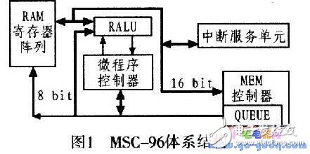
The register array inside the MCU is connected to the RALU through a controller and two buses. The two buses are 8-bit A-BUS and 16-bit D-BUS. DBUS is only used for data transmission between RALU and registers, while A-BUS is used as the address bus in the above-mentioned transmission process. When MCU accesses on-chip and off-chip registers through the register controller, A-BUS can be used as a multiplexed address/data bus.
1.2 A8096 overall structureIn order to reduce area and power consumption, A8096 adopts hard-wired logic control mode to replace the above-mentioned microprogram controller. According to the MSC-96 architecture, the main functional modules of A8096 include: IPU (InSTructiON Pre-fetch Unit. Instruction prefetch unit), CU (Control Unit, control unit), ALU (ArithmeTIC Logical Unit, arithmetic logic unit), MEM_C- TRL (MEM controller), RF_CTRL (register file controller), ISR (Interrupt Service RouTIne unit, interrupt service unit), GPIO (General Purpose Input Out-put, general purpose input output unit) and other main functional components. Its structure is shown in Figure 2.
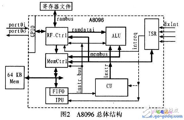
A8096 uses 3 buses: one is MEM bus, used for IPU and MEM CTRL to read and write control of program space and data space; 16 bit data line, 16 bit address line, read and write signal memrd/memwr; one is internal The Register File bus is used for RF_CTRL to read and write access to the internal register array. The address line is 8 bit, the data line is 16 bit, the read and write signals are rf_rd/rf_wr; one is the SFR bus, which is used to access data The space address is in the specially defined register space of 00H~19H. 8-bit address bus, 16-bit data bus, read and write signals sfrrd/sfrwr. In addition, the data interaction between IPU and MEMCTR is completed through the 8-bit data line instr_bus, and its function is to transfer instructions from the prefetch instruction queue to the CU unit, etc.
2 MCU design and implementation 2.1 MCU working principleA8096 prefetches instructions through the IPU (instruction prefetch unit) and stores them in the prefetch instruction queue. The CU (control unit) fetches instructions from the IPU instruction queue and decodes them to generate signals such as control timing. ALU unit, RAM controller, MEM controller and other components have decoding modules, which actively work according to the current instruction and the current instruction cycle. For example, the RAM controller fetches the operand in the corresponding cycle of the addition instruction and sends it to the ALU unit, and the ALU receives the data in the corresponding cycle, then performs operations and outputs the result.
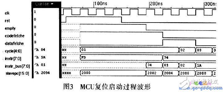
2.2 MCU startup processAt power-on reset, the MCU is in the reset state (rst signal is valid). When reset, the instruction queue in the IPU unit is cleared (empty signal is valid), the bus is in the idle state, and the IPU immediately performs instruction prefetching. The first address (2080H) instruction of the program space is fetched from the instruction queue, and then the queue empty signal ( empty) is invalid, and the command is sent out (instr_bus) at the same time. At the same time as reset, the instruction fetch signal (codefetche) of the control unit (CU) is always valid. After the empty signal of the instruction queue is invalid (CU waits until empty is invalid), the instruction enters the CU through the instr_bus, and the instruction opcode It is stored in the instruction register, as shown in Figure 3, the instr register is updated to the opcode 74 of the addition instruction. At this point, the MCU has completed the reset, automatic instruction fetching operation, and started to execute the instruction down, and the IPU unit will also continue the instruction prefetching operation.
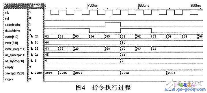
In A8096, there are two levels of instruction prefetch concept: the first level is the instruction pre-unit IPU using bus idleness to continuously prefetch instructions from the program space and store them in the instruction queue; the first level is the instruction prefetch during instruction execution, when a When the instruction is executed to the last clock cycle, the CU unit will send an instruction fetch signal to perform the prefetch instruction at the instruction execution level, and the opcode of the next instruction will be prefetched (wait when the instruction queue is empty), and Decode immediately to determine the byte length of the instruction and the number of instruction execution cycles.
As shown in Figure 4, in the last cycle of the addition instruction (cycle=05), the instruction fetch signal codefetche of the CU unit is valid, and the opcode (6C, multiplication opcode) of the next instruction is pre-fetched, and the table lookup is performed at the same time Decoding determines the length of the instruction byte and the number of instruction cycles, and then the opcode is stored in the instruction register instr (at this time, the instruction cycle counter cycle starts counting from 01). The operands of the subsequent multiplication instructions will also be continuously fetched for execution until the last cycle of the multiplication instruction, and the opcode of the next instruction will be prefetched.
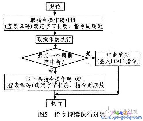
Need to explain: codefetche is the operation code signal, and datafetche is the operand signal. If there is an interrupt request in the last cycle of the instruction, insert the LCALL instruction for interrupt processing and read the next instruction. The process is shown in Figure 5.
In the MCU design process, first complete the instruction analysis of each instruction, determine the action to be done in each cycle, and then each component decodes the relevant instruction according to the instruction analysis table (the RAM controller only interprets the action that the RAM needs to do) , ALU only translates the actions that ALU has to do). The process is described as follows: When prefetching the opcode, the CU unit decodes the opcode to determine the byte length (nr_bytes) and the number of instruction cycles (nr_cycles) of the instruction. Then the CU fetches the operand according to the instruction byte length (nr_bytes), and other components execute the corresponding instruction operation according to the instruction and the current instruction cycle (curcycle). Table 1 is the analysis table of the addition instruction. The decoding process of the addition instruction is used to illustrate the entire decoding process:
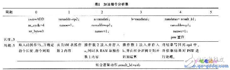
1) Addition instruction ADD OPl OP2 (write the result of OPl+0P2 into OPl); its object code format is: ADD OP2 OPl, where OPl and OP2 are operand addresses.
2) Cycle 0 actually refers to the last clock cycle of the previous instruction. In this cycle, the codefetche fetch signal is valid, and the IPU unit sends the instruction to the CU unit to determine the instruction cycle and instruction length.
3) The l cycle fetch operand signal datafetche is valid, op2 (address) comes in, is sent to the RAM address line, and sends a read signal (fetch operand 2 from the RAM register array).
4) 2 cycles operand 2 is taken in and stored in the a register in the ALU; this cycle takes the operand signal datafetche valid, opl (address) comes in, is sent to the RAM address line, and sends a read signal.
5) The 3-cycle operand l is taken in and stored in the b register in the ALU; the adder immediately performs a+b operation.
*The cycle puts the result of the addition on the RAM data line, the address line = opl, and sends a write signal. Write the addition result back to opl, and process the PSW according to the result.
7) 5 cycles of no action, used for the process of write back operation.
3 Verification results 3.1 Simulation verificationThe function and structure design of the chip is only a part of the design process. In order to ensure the success of the final design, it must be fully simulated and functionally verified. The testing methods for MCU are as follows: 1) Unit testing of functional modules to verify the functional correctness of the modules, including interface timing and so on. 2) System integration test, first write a simple machine code test vector for preliminary debugging: then use a compiler to write an assembler program and compile it into binary machine code for program function testing. In the integration test, compile assembly test programs, compile them into machine code with a compiler, and run these test programs under Cadenee NC for simulation testing. Various addressing modes are tested for each instruction, and the test program automatically writes the test result to the DEBUG register to facilitate debugging. After complex testing and continuous correction, the verification result shows the correctness of the MCU instruction execution.
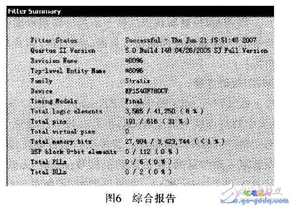
3.2 FPGA verificationThe FPGA device used is Stratixâ…¡ model EP1S40F780C7. The comprehensive result shows: A8096 uses 3 565 LE (LogIC Element). Timing analysis results: A8096 can run at a clock frequency of 49.93 MHz. The distribution of FPGA resources occupied by A8096 is shown in Figure 6.
In this design, the hard-wired control logic in RISC technology is used to reduce MCU area, reduce power consumption, and improve MCU execution efficiency. FPGA implementation shows that it only occupies 3 565 LE units and the working clock can reach 50 MHz. At the same time, the MCU has strong scalability and practicability, and has a wide range of applications. It can be easily connected to timers, serial communication interfaces (I2C), serial peripheral interfaces (SPI), analog-to-digital (A/D) converters and other peripherals. The functional units constitute various embedded systems, which are fully of practical application value.
Shenzhen Hongyian Electronics Co., Ltd. , https://www.hongyiancon.com