This is a special differential amplifier with ultra-high input impedance, extremely good CMRR, low input offset, and low output impedance that can amplify signals at common-mode voltages.
With the rapid development of electronic technology, operational amplifier circuits have also been widely used. The instrumentation amplifier is a precision differential voltage amplifier that is derived from an operational amplifier and is superior to an operational amplifier. The instrumentation amplifier integrates key components into the amplifier. Its unique structure makes it highly common mode rejection ratio, high input impedance, low noise, low linearity error, low offset drift gain setting flexibility, and ease of use, making it in the data Acquisition, sensor signal amplification, high-speed signal conditioning, medical instruments, and high-end audio equipment are all highly favored. The instrumentation amplifier is a closed-loop gain component with a differential input and a single-ended output at the opposite reference. It has a differential input and a single-ended output at the opposite reference. Unlike an op amp, the op amp's closed-loop gain is determined by the external resistor connected between the inverting input and the output, while the instrumentation amplifier uses an internal feedback resistor network that is isolated from the input. The input signal is applied to the two differential inputs of the instrumentation amplifier. The gain can be preset internally or can be preset by the user through internal pins or through an external gain resistor that is isolated from the input signal.
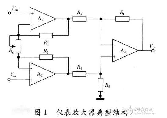
Instrumentation amplifier construction principleThe typical structure of the instrumentation amplifier circuit is shown in Figure 1. It is mainly composed of a two-stage differential amplifier circuit. Among them, the op amps A1, A2 are in-phase differential input mode. The non-inverting input can greatly increase the input impedance of the circuit and reduce the attenuation of the weak input signal; the differential input can make the circuit only amplify the differential mode signal, and The mode input signal only acts as a follower, so that the ratio of the magnitude of the difference mode signal to the common mode signal (ie, the common mode rejection ratio CMRR) is improved. In this way, in the differential amplifier circuit composed of the operational amplifier A3 as the core component, the accuracy matching requirements for the resistors R3 and R4, Rf and R5 can be significantly reduced under the same CMRR requirement, so that the instrumentation amplifier circuit is simpler than the differential. The amplifier circuit has better common-mode rejection capability. Under the condition of R1=R2, R3=R4, and Rf=R5, the gain of the circuit of FIG. 1 is: G=(1+2R1/Rg)Rf/R3. It can be seen from the formula that the circuit gain can be adjusted by changing the Rg resistance.
â— High common mode rejection ratio
The common-mode rejection ratio (CMRR) is the ratio of the differential-mode gain (A d) to the common-mode gain (Ac), that is: CMRR = 20 lg | Ad/ Ac | dB; the instrumentation amplifier has a high common-mode rejection ratio, CMRR typical The value is 70 to 100 dB or more.
â— High input impedance
The instrumentation amplifier must have a very high input impedance, and the in-amp and inverting input impedances of the instrumentation amplifier are very high and well balanced with each other. The typical value is 10^9~10^12Ω.
â— Low noise
Since the instrumentation amplifier must be able to handle very low input voltages, the instrumentation amplifier cannot add its own noise to the signal. At 1 kHz, the input noise referred to the input is less than 10 nV/Hz.
â— Low linearity error
Input offset and scale factor errors can be corrected by external adjustments, but linearity errors are inherent to the device and cannot be eliminated by external adjustments. The typical linearity error of a high-quality instrumentation amplifier is 0.01%, and some even lower than 0.001%.
Low offset voltage and offset voltage drift
The offset drift of the instrumentation amplifier also consists of input and output. The input and output offset voltages are typically 100μV and 2mV, respectively.
Low input bias current and offset current error
The base current of the bipolar input op amp and the gate current of the FET input op amp generate an offset error when this bias current flows through the unbalanced signal source resistor. Bipolar input instrumentation amplifier bias current is typically 1 nA ~ 50 pA; and FET input instrumentation amplifier bias current at room temperature is typically 50 pA.
â— Abundant bandwidth
Instrumentation amplifiers provide sufficient bandwidth for specific applications. Typical unity-gain small-signal bandwidths are between 500 kHz and 4 MHz.
â— With "test" and "reference"
Instrumentation amplifiers are also unique with "detect" and "reference" terminals allowing remote sensing of the output voltage while minimizing the effects of internal resistor drop and ground drop (IR).
The output impedance of a signal source is often several kΩ or more, so the input impedance of the instrumentation amplifier is very large—usually a few GΩ, and it operates between DC and about 1MHz. At higher frequencies, the problem of input capacitive reactance is greater than the input impedance. Differential amplifiers are often used in high-speed applications. Differential amplifiers are faster but have lower input impedance.
Op Amp's key parameters
When the design engineer determines the amplifier, the main concern is the supply current, -3dB bandwidth, common-mode rejection ratio (CMRR), input voltage compensation and offset voltage drift, noise (refer to input), and input bias current.
The internal structure of the three op amp instrumentation amplifier
Most instrumentation amplifiers use three op amps in two stages: a preamplifier consisting of two op amps followed by a differential amplifier (Figure 1a). Preamplifiers provide high input impedance, low noise, and gain. The differential amplifier rejects common-mode noise and can also provide some additional gain when needed.
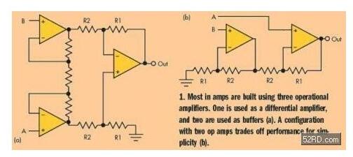
figure 1
Two op amp instrumentation amplifier structure
The structure can be replaced with fewer components with two op amps (Figure 1b), but with two drawbacks. First of all, the asymmetric structure makes the CMRR lower, especially at high frequencies. Second, due to the limited amount of gain in the first stage. The output error is fed back to the input, resulting in greater input-related noise and compensation errors.
How to protect the instrumentation amplifier's input from overvoltage?
Designers need external current limiting resistors to prevent overvoltages from driving excessive current through internal electrostatic discharge (ESD) clamp diodes. The value of these resistors depends on the instrumentation amplifier's noise level, supply voltage, and required overvoltage protection. See the device datasheet for recommended values.
These resistors add noise, so an alternative solution is to use an external high-current clamp diode and very small resistance. Unfortunately, the leakage current of most common diodes is too large and can cause large output drift errors that increase exponentially with temperature. Designers should not use standard diodes for high-impedance signal sources.
What is RFI rectification? How to prevent?
Long leads between the sensor and the instrumentation amplifier can cause RF. The instrumentation amplifier then rectifies this RF to a DC offset. Figure 2 shows a scheme that filters out RF before it reaches the instrumentation amplifier. The elements R1a and C1a form a low-pass filter at the non-inverting terminals, and R1b and C1b also constitute a low-pass filter at the inverting terminals.
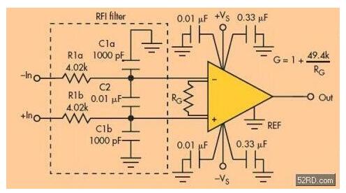
figure 2
A good match of the cutoff frequencies of these two low-pass filters is important. Otherwise, the common-mode signal will be converted to a differential signal. C2 will “short-circuit†the input at high frequencies, which can reduce this requirement to some extent. The size of C2 should be at least 10 times that of C1.
Nonetheless, the matching of C1a and C1b is still critical, and a ±5% C0G film capacitor should be used. The differential bandwidth of this filter is [1/2πR(2C2+C1)] and the common-mode bandwidth is [1/2πR1C1]].
What are the pros and cons of buying a monolithic amplifier and building an instrumentation amplifier with an op amp?
The main reason for building an instrumentation amplifier with discrete op amps is that the required instrumentation amplifiers are not available in the market. There are more than 5,000 types of op amps produced by different manufacturers, and there are only about 100 instrument amplifier models.
However, if you can find a monolithic instrumentation amplifier that meets the performance requirements, use it instead of building it yourself. In this way, development time is saved, and the size of a single piece of components is certainly small.
In addition, CMRR performance will be better. Since most resistors are on-chip, board parasitics are much smaller. Another advantage is that the monolithic design noise and bandwidth parameters are generally better for any rated current.
Three op amp measurement (instrument) amplifier internal circuit analysis
In many test situations, the output signal of the sensor is often very weak, and it is accompanied by a large common-mode voltage (including interference voltage). Generally, a measurement amplifier is used for this signal.
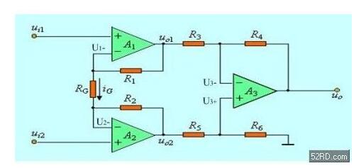
The figure above is a widely used three-op amp measurement amplifier circuit. The measurement amplifier circuit also has a gain adjustment function, and adjusting RG can change the gain without affecting the symmetry of the circuit. Among them, A1 and A2 are two general-purpose integrated operational amplifiers with the same performance (mainly input impedance, common-mode rejection ratio, and open-loop gain). They work in the same-phase amplification mode and form a balanced and symmetrical differential amplifier input stage. A3 works poorly. The dynamic amplification method is used to further suppress the common mode signals of A1 and A2, and is connected to a single-ended output mode to meet the needs of a grounded load.
The circuit is analyzed as follows:
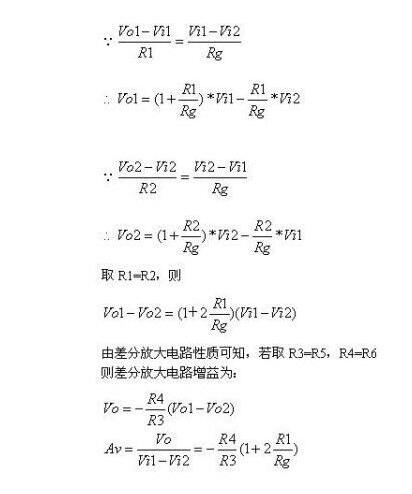
The common-mode rejection ratio of the measurement amplifier mainly depends on the symmetry of the input stage amplifiers A1 and A2, the common-mode rejection ratio of the output stage op amp A3, and the matching accuracy of the output stage external resistors R3, R5 and R4 and R6 (±0.1% Within. The common mode rejection ratio can reach more than 120dB.
In addition, the measurement amplifier circuit also has a gain adjustment function, and adjusting RG can change the gain without affecting the symmetry of the circuit. And because the input stage uses a symmetrical in-phase amplifier, the input resistance can reach hundreds of megaohms or more.
At present, many companies have developed a variety of high-quality monolithic integrated measurement amplifiers, usually only an external resistor RG is used to set the gain, few external components, and flexible use, capable of handling voltage signals from a few microvolts to several volts.
Dongguan Yijia Optoelectronics Co., Ltd. , https://www.everbestlcdlcm.com