In the layout of the IC layout, the Design Rules will often indicate that the metal line should be dug when the metal line is larger than a certain width. At the same time, the metal density will also be limited. If less than the specified percentage, add dummy metal. The two rules are aimed at the same purpose, that is, the uniformity of the metal on the entire chip.
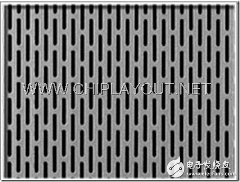
Imagine the density of metal on the chip is not uniform enough, some places have high density, and some places have low density. After metal deposition, the metal density is low, and after etching and polishing, the original layout (Layout)
In areas where the metal density is low, the thickness of the metal corresponding to the wafer is now thinner than the area where the metal density is higher. Therefore, the flatness of the wafer is directly affected, which affects the accuracy of subsequent processes and causes
The poor electrical performance of the IC directly affects the yield of the wafer.
When the metal density of the entire chip layout is too low, the corresponding amount of metal to be etched out on the wafer is too much, which easily causes the etching to be unclean, and there is too much metal remaining on the wafer, which affects subsequent processes. When the metal density of the entire chip layout is too high, the corresponding amount of metal to be etched out on the wafer is small, which easily causes excessive etching, and the normal metal wire is also etched away.
Innosilicon Machine:Innosilicon A10 ETHMaster (500Mh),Innosilicon A10 Pro ETH (500Mh),Innosilicon A10 Pro+ ETH (750Mh),Innosilicon A11 Pro ETH (1500Mh)
Innosilicon is a worldwide one-stop provider of high-speed mixed signal IPs and ASIC customization with leading market shares in Asian-Pacific market for 10 consecutive years. Its IP has enabled billions of SoC's to enter mass production, covering nodes from 180nm to 5nm across the world`s foundries including: GlobalFoundries, TSMC, Samsung, SMIC, UMC and others. Backed by its 14 years of technical expertise in developing cutting-edge IPs and ASIC products, Innosilicon has assisted our valued partners including AMD, Microchip and Microsoft to name but a few, in realizing their product goals.
Innosilicon team is fully devoted to providing the world's most advanced IP and ASIC technologies, and has achieved stellar results. In 2018, Innosilicon was the first in the world to reach mass production of the performance-leading GDDR6 interface in our cryptographic GPU product. In 2019, Innosilicon announced the availability of the HDMI v2.1 IP supporting 4K/8K displays as well as our 32Gbps SerDes PHY. In 2020, we launched the INNOLINK Chiplet which allows massive amounts of low-latency data to pass seamlessly between smaller chips as if they were all on the same bus. With a wide range of performance leading IP in multiple FinFET processes and 22nm planar processes all entering mass production, Innosilicon's remarkable innovation capabilities have been proven in fields such as: high-performance computing, high-bandwidth memory, encrypted computing, AI cloud computing, and low-power IoT.
Innosilicon Machine,A11 Pro 1500M Miner,Asic Miner A11 Pro 8G,A11 Pro 8G 1500Mh,ETC miner
Shenzhen YLHM Technology Co., Ltd. , https://www.asicminer-ylhm.com