1 Introduction The diversity of fieldbus provides more choices for bus device users, and it also brings compatibility problems between bus devices for bus users. In the process of expansion and reconstruction, the factory may choose products that are different from the original field device bus standards. These devices cannot share data with each other due to the use of different field buses, thus reducing the advantages of complementary functions between devices. Therefore, it is of great practical significance to explore how to solve the interconnection of different fieldbus systems for the objective facts of multiple bus coexistence. This paper mainly studies the principle of protocol conversion between PROFIBUS-DP and CAN, and designs a gateway to realize the interconnection of these two buses.
2 program design
For two heterogeneous fieldbuses, the data link layer and application layer protocols are completely different. To achieve their interconnection, a gateway is required for protocol conversion. Protocol conversion is performed hierarchically in the gateway. The gateway unpacks the data sent by the fieldbus device 1 at different protocol levels, and finally obtains the user data in the message. It is then packaged layer by layer according to Fieldbus Protocol 2 and then sent to the devices in Fieldbus 2.
A gateway is a network interconnection device used to implement a layer above the data link layer. It is equivalent to a protocol converter and can be bidirectional or unidirectional to connect networks of different protocols. It does not require the same protocol for the data link layer and the application layer as the bridge.
The fieldbus gateway usually seen is a single CPU structure. In this structure, the CPU has to complete the transmission and control of the two kinds of bus information, and at the same time, to complete the conversion of the two bus protocols, the CPU load of the scheme is heavy. Control is complex and the software uses multiple nesting. This paper proposes a gateway design method based on dual CPU structure. The two CPUs in the system process and control the data of the two bus protocols, and put the information to be transferred into the dual-port RAM to realize information sharing and Passing, this solution is easy to control, the software is simple, and the burden on the CPU is reduced, and the reliability is enhanced.
3 system hardware design system hardware can be divided into three parts according to the function, one is the CAN bus interface circuit, complete the CAN bus data transceiver and control; the second is the PROFIBUS-DP bus interface circuit, complete the PROFIBUS bus data transmission and reception and control The third is a dual-port RAM interface circuit for completing the exchange of two bus data.
3.1CAN bus interface hardware structure
The overall hardware structure of the CAN bus interface is shown in Figure 1. The circuit is mainly composed of four parts, a microcontroller 89C52 (1), an independent CAN communication controller SJA1000, a CAN bus transceiver 82C250 and a high speed photocoupler 6N137.
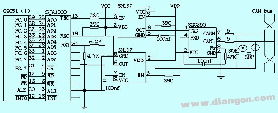
89C52 (1) is responsible for the initialization of SJA1000, through the control of SJA1000 to achieve data reception and transmission and other communication tasks, but also responsible for the data exchange with the PROFIBUS bus interface side, select 89C52 (1) as the CPU mainly because it is not only with CAN The control chip SJA1000 is compatible, and the internal integrated 8kflashRAM can meet the storage requirements of the system, and no need to expand the program memory.
SJA1000 is a CAN bus controller. It is a stand-alone CAN controller that is an alternative to PHILIPS' CA82C200CAN controller, which is compatible with the PCA82C200 in both software and pins. It has two working modes, BasicCAN and PeliCAN, among which BasicCAN is compatible with PCA82C200; PeliCAN is an extended feature mode that supports CAN2.0B protocol with many new features. The main new features of SJA1000 are: standard structure and extended structure message reception and transmission; 64-byte receive FIFO; standard and extended frame formats have single/dual receive filters with receive mask and receive code registers; / write access error counter; programmable error alarm limit; last error code register; every CAN bus error can generate error interrupt; lost arbitration interrupt with lost arbitration positioning function; single shot mode when error occurs or is lost It is not retransmitted during arbitration; it only listens to the CAN bus without answering no error flag; it supports hot swapping without interference software drive bit rate detection; hardware disables CLKOUT output.
The AD0-AD7 of the SJA1000 is connected to the P0 port of the 89C52(1), the CS is connected to the P2.7 of the 89C52(1), and the CPU off-chip memory address of P2.7 is 0. The SJA1000 can be selected by the CPU. The SJA1000 performs the corresponding read and write operations. The RD, WR, and ALE of the SJA1000 are respectively connected to the corresponding pins of the 89C52.
In order to enhance the anti-interference ability of the CAN bus node, the TX0 and RX0 of the SJA1000 are not directly connected to the TXD and RXD of the 82C250, but are connected to the 82C250 through the high-speed optocoupler 6N137, thus achieving good CAN nodes on the bus. The electrical isolation between the two power supplies VCC and VDD used in the optocoupler part of the circuit is completely isolated. In addition, the interface part of 82C250 and CAN bus also adopts certain safety and anti-interference measures. The CANC and CANL pins of the 82C250 are connected to the CAN bus through a 5Ω resistor to provide a current limiting function to protect the 82C250 from overcurrent. Two 30P small capacitors are connected in parallel between CANH and CANL and ground. It can filter high frequency interference on the bus and certain anti-electromagnetic radiation. In addition, between the two CAN bus access terminals and ground A protection diode is connected in reverse. When the CAN bus has a high negative voltage, a short circuit through the diode can provide a certain overvoltage protection. A slope resistor is connected to the Rs pin of the 82C250.
3.2 PROFIBUS-DP bus interface circuit
The hardware circuit of the PROFIBUS-DP bus interface is also composed of four parts, the microcontroller 89C52 (2), the PROFIBUS-DP communication controller protocol chip SPC3, the optocoupler HCPL7101 and 6N137, and the RS485 bus drive circuit. Figure 2 is a hardware circuit diagram of the PROFIBUS-DP communication controller to the RS485 bus driver.
89C52 (2) is mainly responsible for controlling SPC3, realizing the conversion and sharing of PROFIBUS-DP bus data.
SPC3 has integrated the data transmission and reception function of the PROFIBUS-DP physical layer, which can independently process the PROFIBUSDP protocol. In addition, SPC3 also integrates 1.5k dual-port RAM as the interface between SPC3 and user program, and AT89C52(2) can be used. SPC3 internal RAM access.
Although SPC3 has integrated the data transfer function of the physical layer, it does not have the RS-485 drive interface, so the RS-485 drive circuit has been added. 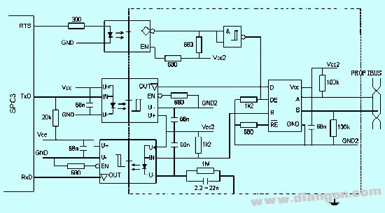
In addition, in order to avoid the influence of the signal on the bus on the circuit, optical isolation is used between the SPC3 and the RS485 bus drive circuit. The TxD and RxD signal isolation devices use Hewlett Packard's 12M high-speed optocoupler HCPL710, and the RTS signal isolation device uses 6N137.
3.3 Dual Port RAM Interface Circuit The sharing and transfer of two bus data is realized by dual port RAM. The device IDT7130 is selected in the system. It is a high speed 1K dual port static RAM. The device provides two independent ports with independent control, address and I/O pins, and allows independent asynchronous read and write access to any address in the memory. The automatic power management features are controlled by the CE, allowing each on the chip. A port circuit enters a very low power mode. The on-chip bus arbitration circuit of IDT7130 has two bus arbitration modes, BUSY and INT. Based on the type of microcontroller used, an interrupt arbitration scheme is used in the system. This method works by assigning a memory address (mailbox or information center) to each port. The left port's interrupt flag is declared to be when the right port is written to the memory address 3FEH, and the left port clears the interrupt by accessing the 3FE memory address. Similarly, when the left port writes the memory address 3FFH, the right port flag is declared. In order to clear the interrupt flag, the right port must access the memory address 3FFH, and the contents of the 3FE and 3FF units in the system give a new meaning, that is, define two Codes 0FFH and 00H. Where 0FFH means sending the command to ask the other party to transmit data, and 00H means sending the data requested by the other party. The connection between the two CPUs and the dual port RAM in the system is shown in Figure 3. The remaining memory cells of the dual port RAM are divided into four parts, of which 0000 units of 0000H-00FFH are used to store data or addresses uploaded by the CAN bus, and two adjacent units are used to store a CAN substation. Data information; 0100H-01F9H These 250 units are used to store the data or address uploaded by the PROFIBUS bus, the adjacent two units are used to store information of a PROFIBUS substation, and the 03FCH unit is used to store the CAN bus equipment to be read. The ID number of the PROFIBUS station, the 03FDH unit is used to store the ID number of the CAN station to be read by the PROFIBUS bus device.
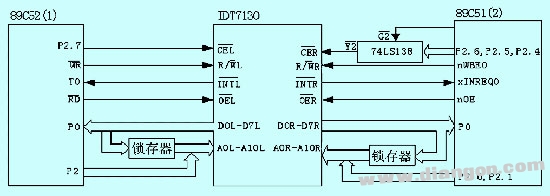
It can be seen from the figure that the mapping address of the dual port RAM in the microprocessor responsible for CAN bus communication is 0x7C00H-0x7FFFH, and the mapping address of the microprocessor responsible for PROFIBUS bus communication is 0x2C00H-0x2FFFH.
4 system software design gateway software can be divided into two parts, one part is responsible for CAN bus data communication, the other part is responsible for PROFIBUS bus data communication.
Each side of the program can be divided into three sub-modules according to the function: protocol chip initialization program, accept data acceptance sub-program, data transmission sub-program. The data accepting subroutine tests the external interrupt to trigger execution. The CAN bus interface side program of the gateway is taken as an example to list the program flow chart, and the interface program on the PROFIBUS side is similar, and will not be described again.
The initialization and transmission procedure of the CAN bus side is shown in Figure 4:
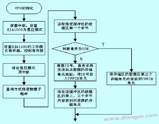
Because the initialization of SJA1000 can only be done in reset mode, the program first masks the SJA1000 interrupt, puts it into reset mode, and then initializes it. The initialization content mainly includes the setting of the working mode, the setting of the acceptance filtering mode, the setting of the acceptance mask register and the acceptance code register, the setting of the baud rate parameter, and the setting of the interrupt enable register. After the SJA1000 completes the initial setup, it is returned to the working state for normal communication tasks.
In the accepting subroutine, the system accepts the data transmitted by the CAN substation by query, and the gateway judges whether the real data is accepted by accepting the content of the first byte of the buffer data area, or sends it to the PROFIBUS-DP site. Send a data request. If the first byte of the data area is 00H, the data information is transmitted, so the storage unit corresponding to the station is obtained according to the ID lookup table, and the second and third bytes of the data area are stored in the unit. At the same time, put the ID in 7FFCH, tell the other party to send the data of the site number; if the content of the byte is FFH, it means that the data request is sent, and the second byte of the data area stores the site number that is required to send the data. Put him in the 7FFCH.
CAN bus interface send data subroutine flow chart shown in Figure 5:
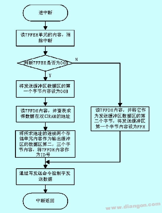
The above sending program is triggered by the interrupt signal of the dual port RAM. After receiving the interrupt signal, the content of the 7FFEH unit is first read, the interrupt signal is cancelled, and then the data stored in the dual port RAM is determined according to the content of the unit. , or the ID number of the CAN substation that is required to send data. If the content of 7FFEH is 00H, it means that the data to be sent to the CAN substation is normal, so the first byte of the transmission buffer is set to 00H, the CAN substation is sent as data, and then the 7FFDH unit content is read. Check the table to find the address of the data in the dual-port RAM, and take two bytes from the address to the second and third bytes of the SJA1000 output buffer data area, and use 7FFDH as the transmitted ID number. If 7FFDH is FFH, it means that PROFIBUS-DP sends the site number of the CAN substation that is required to send data, so just put it in the second byte of the SJA1000 transmit buffer data area and put the first one The byte is set to FFH to inform the CAN site that the transmitted data is the ID number. After the above work is completed, the data is finally sent by writing a command word.
5 Conclusion
Practice has proved that the two-way gateway with dual CPU structure can complete the task of CAN bus to PROFIBUS-DP bus protocol conversion, and solves the problems of low data transmission rate and poor data transmission reliability in the single CPU structure gateway. CAN bus and PROFIBUS-DP bus protocol conversion requirements. It connects the CAN bus device with the PROFIBUS bus device, so that the two field bus devices can communicate efficiently, and finally achieve the purpose of data sharing and function complementation. Moreover, the staff does not have to care about the entire contents of the two bus physical layers and data link layers during use, which brings great convenience to the research and development of the bus products. In addition, the design scheme of the dual CPU structure has reference significance for the gateway design between other field buses, and is a method worthy of promotion.
Capacitor Motor,Furnace Capacitor,Start Capacitor,Capacitor Start Motor
Wentelon Micro-Motor Co.,Ltd. , https://www.wentelon.com