[Introduction] At present, the speed of the digital design system is measured in GHz, and the challenge of this speed is far more significant than in the past. Since the edge rate is measured in picoseconds, any impedance discontinuity, inductive or capacitive interference can adversely affect signal quality. Although there are various sources that cause signal interference, a particularly often overlooked source is vias.
Over the years, engineers have developed several methods to deal with the noise that causes distortion of high-speed digital signals in PCB designs. As design technology keeps pace with the times, the technical complexity of our response to these new challenges is increasing. At present, the speed of digital design systems is measured in GHz, and the challenge of this speed is far more significant than in the past. Since the edge rate is measured in picoseconds, any impedance discontinuity, inductive or capacitive interference can adversely affect signal quality. Although there are various sources that cause signal interference, a particularly often overlooked source is vias.
Hidden dangers in simple vias
Over-hole signals in high-density interconnect (HDI), high-level printed circuit boards, and thick back/intermediate boards are subject to more jitter, attenuation, and higher bit error rate (BER), causing data to be received at the receiving end. Misinterpretation.
Take the backplane and daughter card as an example. When impedance discontinuities are encountered, the focus is on the connectors between these boards and the mother card. Typically, these connectors are very matched in impedance and the discontinuities actually originate from the vias.
As the data rate increases, the amount of distortion caused by the plated through hole (PTH) via structure also increases - typically at an exponential rate that is much higher than the associated data rate increment. For example, the distortion of a PTH via at 6.25 Gb/s is typically more than twice that of the distortion produced at 3.125 Gb/s.
Unwanted via stub extension layers appearing on the bottom and top layers, making the vias appear as lower impedance discontinuities. One way engineers can overcome the extra capacitance of these vias is to minimize their length and thus reduce their impedance. This is the origin of the back drill.
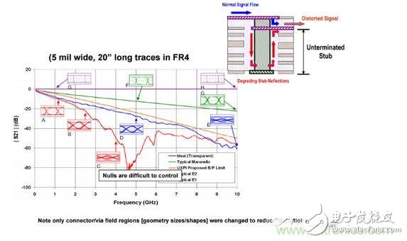
Long over-hole residual signal distortion [1]
Using back drilling technology
Back-drilling has been widely recognized as a simple and effective way to minimize channel signal attenuation by eliminating via stubs. This technology is called deep drilling and it uses traditional numerical control (NC) drilling equipment. At the same time, the technology can be applied to any type of board, not just thick boards like backplanes.
The drill bit used in the back drilling method is slightly larger in diameter than the original via to remove unwanted conductor stubs. The drill is typically 8 mils larger than the main drill specification, but many manufacturers can meet more stringent specifications.
It is important to remember that the distance between the trace and the plane needs to be large enough to ensure that the back-drilling program does not penetrate nearby traces and planes. To avoid penetration of traces and planes, a pitch of 10 mils is recommended.
In general, there are many benefits to reducing the length of a via stub by back drilling, including:
Decreasing deterministic jitter by orders of magnitude results in lower bit error rates.
Reduce signal attenuation with improved impedance matching.
Reduce electromagnetic interference/electromagnetic compatibility radiation from stubs and increase channel bandwidth.
Reduce the resonant excitation mode and crosstalk between vias.
Reduce manufacturing and layout impact with a lower manufacturing cost than sequential lamination.
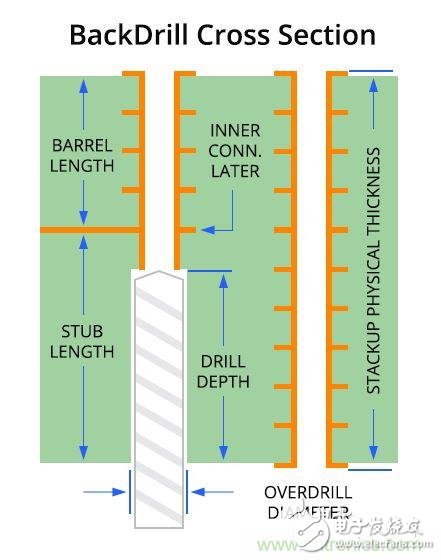
Back drill cross section
Communicate design intent through backsprint
This approach also brings reliability issues as back-drilling technology is used frequently in high-density interconnects and high-speed design applications. Some of these issues include lack of design guidelines, manufacturing tolerances, and how to ensure that design intent is communicated well to manufacturing units.
So, how do you ensure that your manufacturer has all the information you need to back-drill target vias and plated through-hole components? How to keep track of multiple levels of back-drilling specifications throughout the design process?
What you need is very simple: a simple visual configuration tool integrated into the design rules allows you to specify different back-drill configurations for the selected objects. Then, let you know which vias need to be back-drilled to help you work.
Outdoor Fixed LED Display is a popular product for its high quality, every year sold to at least 80,000 pieces around the world, including Europe, North America, southeast Asia.Compared to other indoor LED display in the market, its biggest advantage is that it can display high-definition images while maintaining low power consumption.Besides, it adopts Die casting aluminum cabinet which is ultra-thin and ultra-light and owns good heat dissipation.Easy to install and maintain and suitable for multiple indoor scenes.
Application:
* Business Organizations:
Supermarket, large-scale shopping malls, star-rated hotels, travel agencies
* Financial Organizations:
Banks, insurance companies, post offices, hospital, schools
* Public Places:
Subway, airports, stations, parks, exhibition halls, stadiums, museums, commercial buildings, meeting rooms
* Entertainments:
Movie theaters, clubs, stages.
Outdoor Fixed LED Display,Led Wall Display Screen,Curved Led Display Screen,Led Display Board
Guangzhou Chengwen Photoelectric Technology co.,ltd , https://www.cwleddisplay.com