This article is mainly about the related introduction of the RF driver amplifier, and focuses on the detailed analysis and description of the design of the RF driver amplifier.
The RF driver amplifier isThe RF driver stage amplifier is a power amplifier that is placed in front of the final stage power amplifier to amplify the input signal to achieve the input power required by the final stage power amplifier.
In the pre-stage circuit of the transmitter, the power of the radio frequency signal generated by the modulation oscillator circuit is very small, and it needs to go through a series of amplification, a buffer stage, an intermediate amplifier stage (driver amplifier), and a final power amplifier stage to obtain sufficient radio frequency. After power, it can be fed to the antenna and radiated.
RF amplifierThe radio frequency power amplifier (RF PA) is an important part of various wireless transmitters. In the pre-stage circuit of the transmitter, the power of the radio frequency signal generated by the modulation oscillator circuit is very small, and it needs to go through a series of amplifying a buffer stage, an intermediate amplifier stage, and a final power amplifier stage to obtain enough radio frequency power before it can be fed. Radiate to the antenna. In order to obtain a large enough radio frequency output power, a radio frequency power amplifier must be used.
Classification and usage
The working frequency of the radio frequency power amplifier is very high, but the relative frequency band is relatively narrow. The radio frequency power amplifier generally adopts the frequency selective network as the load loop. Radio frequency power amplifiers can be divided into three types of working states: A (A), B (B), and C (C) according to the current conduction angle. The conduction angle of the class A amplifier current is 360°, which is suitable for small signal low-power amplification. The conduction angle of the class B amplifier current is equal to 180°, and the conduction angle of the class C amplifier current is less than 180°. Both Class B and Class C are suitable for high-power working conditions, and the output power and efficiency of Class C working conditions are the highest among the three working conditions. Most RF power amplifiers work in Class C, but the current waveform distortion of Class C amplifiers is too large and can only be used to amplify the resonant power of the load by using a tuning loop. Due to the filtering capability of the tuning loop, the loop current and voltage are still close to sinusoidal waveforms, and the distortion is small.
Technical Parameters
The main technical indicators of the amplifier:
(1) Frequency range: The operating frequency range of the amplifier is
The premise of road topology design. [1]
(2) Gain: It is the basic index of the amplifier. According to the gain can be determined
The number of stages and device types of the amplifier. G(db)=10log(Pout/Pin)=S21(dB)
(3) Gain flatness and return loss
VSWR "2.0orS11, S22"-10dB [1]
(4) Noise figure: The noise figure of the amplifier is the ratio of the signal-to-noise ratio of the input signal to the signal-to-noise ratio of the output signal, which indicates the deterioration of the signal quality after the signal passes through the amplifier. NF(dB)=10log[(Si/Ni)/(So/No)]
RF amplifier power parameters
In modern wireless communication, the use of radio frequency equipment is quite popular, and radio frequency amplifiers play a vital role in the equipment. The measurement of power parameters in the amplifier has also attracted considerable attention. There are some misunderstandings in the understanding and application of parameters. The following is an amplifier characteristic to illustrate the meaning and application of related power parameters [2].
When describing an amplifier, the basic parameters are gain and maximum output level (power). In order to have a more accurate description of the gain, the parameters of the linear characteristic are introduced to weigh t, usually expressed by the input power corresponding to the ldB compression point and the linear input level. The difference between the two is the input dynamic range of the amplifier. . For the lDB compression point, it is described in the GSM repeater standard YD Ting 952-1998: The output power of the lDB compression point refers to the input power corresponding to the input power when the gain of the amplifier is reduced by 1db. It means that the actual output power at that time is smaller than the output power corresponding to the ideal linear amplifier by lDB [2].
To further describe linearity. Another indicator is the gain step error, which indicates whether the output changes by the same magnitude when the input changes unit signal strength.
An actual amplifier, due to the influence of physical characteristics and noise, cannot maintain a linear state when the input level is too small. Therefore, the concept of minimum output level is introduced. It is generally considered that the corresponding input level when the output is 3dB higher than the noise level is the minimum input level. The output noise power of the amplifier is: P=kTBGF.
Design of RF Driver AmplifierAt present, 8Vpp and pulse width modulation RF high-voltage/high-power drivers can be realized on the basis of 1.2V 65nm CMOS technology. In the operating frequency range of 0.9 to 3.6GHz, the chip can provide a maximum output swing of 8.04Vpp to a 50Ω load at a working voltage of 9V. This allows CMOS drivers to directly connect and drive power transistors such as LDMOS and GaN. The maximum on-resistance of this driver is 4.6Ω. The duty cycle control range measured at 2.4GHz is 30.7% to 71.5%. By using a new thin oxide layer drain extension MOS device, the driver can achieve reliable high-voltage operation, and this new device does not require additional costs when implemented by CMOS technology.
Modern wireless handheld communication radios (including radio frequency (RF) power amplifiers (PA)) are implemented in deep sub-micron CMOS. However, in wireless infrastructure systems, due to the need for larger output power levels, it is necessary to achieve RF PA through silicon LDMOS or hybrid technologies (such as GaA and more advanced GaN). For the next generation of reconfigurable infrastructure systems In other words, the switch mode PA (SMPA) seems to provide the required flexibility and high performance for multi-band multi-mode transmitters. However, in order to connect the high-power transistors used in the SMPA of the base station to all the digital CMOS modules of the transmitter, a broadband RF CMOS driver capable of generating a high voltage (HV) swing is required. This will not only achieve better high-power transistor performance, but also directly use digital signal processing to control the required SMPA input pulse waveform, thereby improving the overall performance of the system.
Design challenge
The input capacitance of LDMOS or GaN SMPA is usually several picofarads and must be driven by a pulse signal with an amplitude higher than 5Vpp. Therefore, SMPA CMOS drivers must provide high-voltage and watt-level RF power at the same time. Unfortunately, deep sub-micron CMOS poses many challenges to the realization of high-voltage and high-power amplifiers and drivers, especially the extremely low maximum operating voltage (ie, low breakdown voltage caused by reliability issues) and passive passives with large losses. Devices (for example for impedance transformation).
Existing solutions
There are not many methods used to implement high-voltage circuits. Technical solutions (such as multi-gate oxide) that can realize high-voltage tolerance transistors can be used, but the cost is that the production process is expensive, and additional masks and processing steps must be added to the baseline CMOS process, so this solution is not ideal. In addition, in order to reliably increase the high voltage tolerance, a circuit scheme using only standard baseline transistors (using thin/thick oxide devices) can be adopted. In the second method, device stacking or series cathodes are the most common examples. However, the complexity and performance of radio frequency have great limitations, especially when the number of series cathode (or stacked) devices increases to 2 or more. Another way to implement high-voltage circuits is to use drain-extended field effect transistors (EDMOS) in baseline CMOS technology as described in this article.
New solution
The drain extension device is based on smart wiring technology, which benefits from the realization of very fine dimensions in the ACTIVE (silicon), STI (oxide) and GATE (polysilicon) regions, and the ability to use baselines without additional costs Deep sub-micron CMOS technology realizes two high voltage tolerance transistors, PMOS and NMOS. Although the RF performance of these EDMOS devices is actually lower compared to standard transistors using this process, they can still be used in the entire high-voltage circuit due to the elimination of important loss mechanisms associated with other HV equivalent circuits (such as series cathodes). To achieve higher overall performance.
Therefore, the high-voltage CMOS driver topology described in this article uses EDMOS devices to avoid device stacking. The RF CMOS driver adopts a thin oxide layer EDMOS device and is manufactured through a 65nm low standby power baseline CMOS process without additional masking steps or processes. For PMOS and NMOS, the fT measured on these devices exceeds 30GHz and 50GHz, respectively, and their breakdown voltage is limited to 12V. High-speed CMOS drivers have unprecedentedly achieved an output swing of 8Vpp up to 3.6GHz. Such a wide band gap-based SMPA provides driving.
Figure 1 is a schematic diagram of the structure of the driver described in this article. The output stage includes an EDMOS-based inverter. EDMOS devices can be directly driven by low-voltage high-speed standard transistors, which simplifies the integration of the output stage and other digital and analog CMOS circuits on a single chip. Each EDMOS transistor is driven by a tapered buffer (buffer A and B in Figure 1) implemented by three CMOS inverter stages. The two buffers have different DC levels to ensure that each CMOS inverter can operate stably at a voltage of 1.2V (limited by technology, that is, VDD1-VSS1=VDD0-VSS0=1.2V). In order to use different power supply voltages and allow the same AC operation, the two buffers have exactly the same structure and are built into a separate Deep N-Well (DNW) layer. The output swing of the driver is determined by VDD1-VSS0, and any value that does not exceed the maximum breakdown voltage of the EDMOS device can be selected at will, while the operation of the internal driver remains unchanged. The DC level shift circuit can separate the input signal of each buffer.
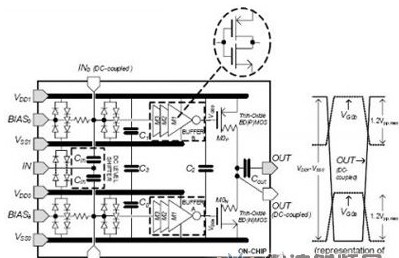
Another function of the CMOS driver is to control the pulse width of the output square wave, which is realized by pulse width modulation (PWM) through variable gate bias technology. PWM control helps to achieve fine-tuning and tuning functions, thereby enhancing the performance of advanced SMPA devices. The bias level of the first inverter (M3) of the buffers A and B can move up/down the RF sinusoidal input signal with reference to the switching threshold of the inverter itself. The change of the bias voltage will change the output pulse width of the inverter M3. Then, the PWM signal will be transmitted through the other two inverters M2 and M1 and combined in the output stage (EDMOS) of the RF driver.
ConclusionThis is the end of the introduction about the RF driver amplifier. If there are any deficiencies, please correct me.
Related Reading Recommendations: Working Principles of RF Amplifiers
Related reading recommendations: Types and structures of RF amplifiers
SHAOXING COLORBEE PLASTIC CO.,LTD , https://www.fantaicolorbee.com