Both 74ls373 and 74hc573 are eight D latches (three states). 74ls373 is a TTL circuit with a supply voltage of 5V. 74hc573 is a CMOS circuit, the power supply voltage working range is 2V ~ 6V. The pin layout of the 74ls373 and 74hc573 is different.
First, the latch 74hc573The 74HC573 is a high-performance silicon gate CMOS device with a transparent latch with eight outputs and a three-state output. The SL74HC573 is the same as the LS/AL573. The device inputs are compatible with standard CMOS outputs, and they are compatible with LS/ALSTTL outputs with pull-up resistors.
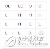
When the latch enable LE is high, the latching of these devices is transparent to the data (ie, the output is synchronized). When the latch enable goes low, data that matches the setup and hold times is latched.
· I/O output can be directly connected to CMOS, NMOS and TTL interfaces
Operating voltage range: 2.0V~6.0V·
Minimum input current: 1.0uA·
High noise resistance of the device · Tri-state bus drive output
Set number of full parallel access
Buffer control input
Enable input hysteresis with improved immunity
When programming:
1. The enable terminal is set to 1, and the output data is consistent with the input data.
2. The enable terminal is cleared to 0, and the output terminal maintains the original value, so that the output data is locked to prevent misoperation.
Truth table and function:
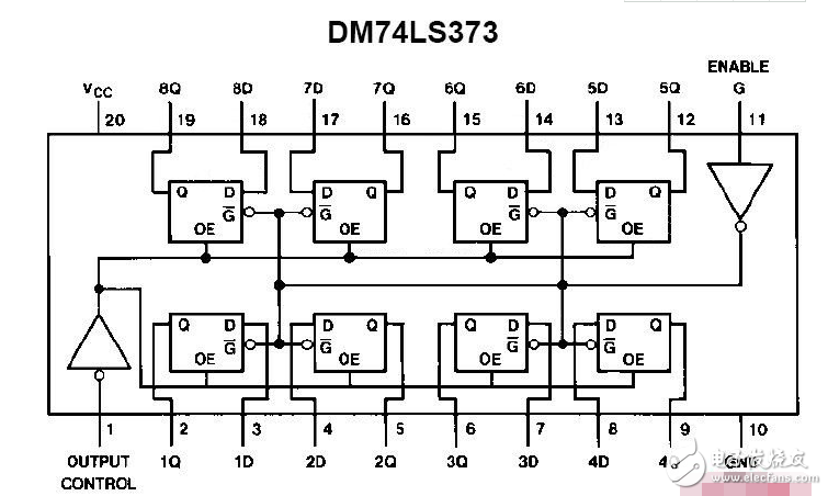
The 74LS373 is a commonly used address latch chip consisting of eight parallel D flip-flops with tri-state buffered outputs. In order to extend the external memory in a microcontroller system, a 74LS373 chip is usually required.  
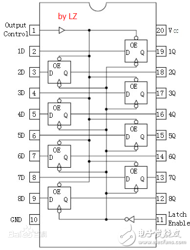
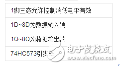
(1).1 pin is output enable (OE), which is active low. When pin 1 is high, regardless of input 3, 4, 7, 8, 13, 14, 17, 18, no matter 11 How the pin (latch control terminal, G), output 2 (Q0), 5 (Q1), 6 (Q2), 9 (Q3), 12 (Q4), 15 (Q5), 16 (Q6), 19 (Q7 ) all exhibit a high-impedance state (or a floating state);
(2). When pin 1 is low, as long as a falling edge appears on pin 11 (latch control terminal, G), output 2 (Q0), 5 (Q1), 6 (Q2), 9 (Q3), 12 (Q4) 15, 15 (Q5), 16 (Q6), and 19 (Q7) immediately present the states of the input pins 3, 4, 7, 8, 13, 14, 17, and 18.
When the latch terminal LE goes from high to low, the 8-bit information at the output is latched until the LE terminal is valid again. When the tri-state gate enable signal OE is low, the tri-state gate is turned on, allowing Q0~Q7 output, and when OE is high, the output is left floating. When the 74LS373 is used as an address latch, OE should be made low. When the latch enable C is high, the output Q0~Q7 states are the same as the input terminals D1~D7; when C is negative During the transition, the input terminals D0~D7 are locked into Q0~Q7. The ALE signal of the 51 MCU can be directly connected to the C of the 74LS373. 74ls373 and microcontroller interface:
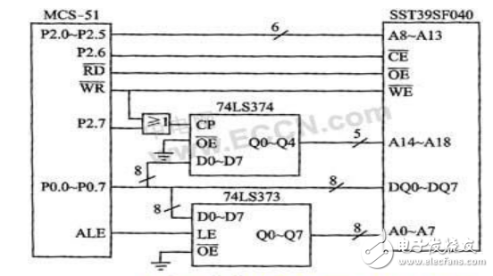
1D~8D is 8 inputs. 1Q~8Q is 8 outputs.
G is the data latch control terminal; when G=1, the latch output is the same as the input; when G changes from "1" to "0", the data is input into the latch.
OE is the output enable end; when OE=“0â€, the tri-state gate is open; when OE=“1â€, the tri-state gate is closed and the output is in a high-impedance state.
In the MCS-51 microcontroller system, the 74LS373 is often used as an address latch. The connection method is shown in the figure above. The input terminals 1D~8D are connected to the P0 port of the single chip microcomputer, the output terminal provides the low 8-bit address, and the G terminal is connected to the address latch enable signal ALE of the single chip microcomputer. The output enable terminal OE is grounded, indicating that the output tri-state gate is always open
Third, the difference between LS and HC1. LS is a low power Schottky and HC is a high speed COMS. The speed of the LS is slightly faster than the HC. HCT input and output are compatible with LS, but low power consumption; F is a high speed Schottky circuit;
2, LS is TTL level, HC is COMS level
3. The LS input is open to a high level, and the HC input is not allowed to open. hc generally requires an upper pull-down resistor to determine the level at which the input is inactive. LS does not have this requirement
4, LS output pull-down strong pull-up weak, HC pull-up pull down the same.
5, the working voltage is different, LS can only use 5V, and HC is generally 2V to 6V;
6, the level is different. LS is a TTL level with low and high levels of 0.8 and V2.4, respectively, while CMOS is 0.3V and 3.6V at 5V, so CMOS can drive TTL, but the reverse is not possible.
7, the driving ability is different, LS generally high level driving capacity is 5mA, low level is 20mA; and CMOS high and low level are 5mA;
8. CMOS devices have poor antistatic capability and are prone to latch-up problems, so CMOS input pins cannot be directly connected to the power supply.
Copper Lugs,Copper Cable Lugs,Plating Copper Cable Lugs,Copper Tube Terminal Lugs
Taixing Longyi Terminals Co.,Ltd. , https://www.longyicopperlugs.com