Why is the efficiency of green LEDs so low, is the carrier injection poor, the Auger loss is large, the internal field is strong, or the material quality is poor? I hope to find the real reason.
Matthias Peter Osram Opto Semiconductors
The LED market for InGaN-based LEDs is at the top of the list. It is the key production material for green and blue light sources and the basis for white LEDs with yellow phosphors.
Although the first InGaN LED is quite dark, its luminous efficiency has increased by more than one order of magnitude over the past decade, and many illuminators are now quite efficient. For example, blue light ThinGaN LEDs manufactured by Osram have a total power conversion efficiency (é¦P) of more than 50%. The design can be applied directly to larger chips without additional losses, such as the 1 x 1mm LED that Osram has introduced, which has a power of 571m/W.
However, the high efficiency of InGaN LEDs is not common, and its output power is lower when the device operates at longer wavelengths. Ultraviolet LEDs have an internal quantum efficiency (IQE) of 80% at lower current densities. When the wavelength is increased, the efficiency is significantly reduced. For example, the IQE at a wavelength of 540 nm is usually less than 30%. The efficiency to the red band is reduced to single digits. Since the "droop" phenomenon is not well understood now, the larger drive current will also reduce IQE, especially for long-wavelength illumination sources.
Red LED manufacturers can solve the problem of InGaN inefficiency by using different material systems, InGaAlP. This proven quaternary material system produces highly efficient yellow, amber and red light sources. Due to carrier limitation, it does not emit light efficiently at wavelengths below 580 nm, which means that there is a "green gap" between 500-580 nm, neither InGaN nor InGaAlP can be prepared. With high efficiency LEDs, this zone has also become a “green light inefficient zoneâ€. LEDs operating in this area have a total power conversion efficiency of less than 20%.
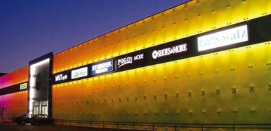
In Regensburg, Germany, the newly renovated K鳃e shopping centre used Osram's LED products in exterior lighting. The lighting system consists of 816 modules, each of which includes a single red, green and blue Golden Dragon LED. Red and blue chips are much more efficient than green chips.
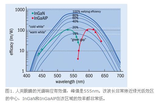
Total power conversion efficiency doesn't mean everything, it's just one of the indicators for evaluating LED performance. If defined by indicators such as performance, luminous flux (lm) or light intensity (cd), the performance of green LEDs will increase, because the human eye's spectral response to green light is stronger than other wavelengths - the human eye's wavelength for 555nm The response is the strongest. Measurements of effectiveness, luminous flux, and light intensity indicate that the green LED emits light at a better quality than the green light inactive region, but we cannot deny that the optical properties in the vicinity of the 560 nm wavelength are poor.
Figure 1 shows that high-efficiency green LEDs can significantly improve the performance of red, green, and blue (RGB) mixed-color white light sources. However, the luminous efficiency of green LEDs is still too low, so that the brightest white light source generally adopts the method of blue light plus phosphor. In this case, we must deal with the Stokes loss caused by the conversion of blue light to yellow light.
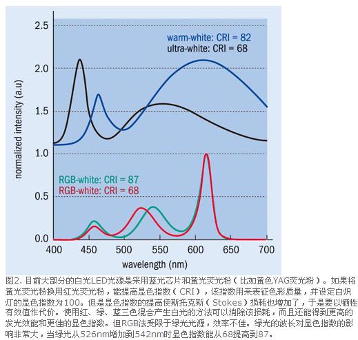
To date, researchers have needed high-efficiency LEDs with emission wavelengths at the center of the green-light inefficiency zone to improve the quality of white light after RGB color mixing (Figure 2).
It is very important to improve the performance of green LEDs. Everyone is trying to find out why InGaN LEDs are less efficient at longer wavelengths. Although various explanations are still in dispute, it is generally accepted that in the manufacture of green LEDs, it requires a higher indium composition than blue light; thus causing major physical changes that make the lattice The constant changes and the band gap is shortened.
LED manufacturers fabricate devices on sapphire or SiC substrates, which will result in dislocations and large strains between the epitaxial layer and the substrate interface, but additional buffer layers can mitigate the effects of dislocations and strain. The strain state of the other layers grown next is only related to the lattice constant of GaN.
The In composition of the blue InGaN quantum well needs to reach 15-20%. Green light requires 25-35%. This does not seem to be a big difference, but it is not. Since InGaN is limited by its solubility, it is difficult to grow a thick layer of a ternary mixture on GaN, especially when the In composition is high. In dissolves the discontinuous region, causing InGaN to separate out two separate phases and form a cluster of In. As for the growth of p-type materials, InGaN's performance at high temperatures also decreases; this hinders the energy band design of the active region barrier layer, so that the transport of carriers is not optimized, and the strain conditions are not improved. To improve.
To produce a high quality InGaN layer, the critical thickness cannot be exceeded, otherwise the material structure will not be tight enough. The critical thickness of the GaAs/InGaAs and GaAs/AlGaAs combinations is relatively easy to determine, but InGaN is different because it is difficult to detect when the dislocations in the InGaN epitaxial layer exceed the usual 108/cm2. However, there is no indication that the green InGaN quantum well exceeds the critical thickness—the X-ray diffraction inverse spatial scan shows that the green quantum well is in full strain state, that is, the critical thickness has not yet been reached.
Increasing the amount of indium in the InGaN quantum well enhances the internal piezoelectric field, which in turn reduces the overlap of electron and hole wave functions. This can be explained by the fact that the traditional InGaN LED has a blue shift in the peak wavelength of the light at high drive currents. The reduction in the overlap of the wave functions does not quantitatively account for the halving of the efficiency of the green and blue LEDs, nor does it explain the efficiency loss mechanism of the high-indium component non-polar LEDs at high current densities.
Professor Fred Schubert of the Institute of Technology (RPI) led a research team who recently explained the reduction in efficiency of InGaN LEDs, focusing on carrier injection. In the conventional LED, since the energy band generated by the internal piezoelectric field is bent, the carriers need to cross the barrier, and the band bending is enhanced as the composition of the indium increases. It can therefore explain why green LEDs are less efficient and perform worse at high currents.
However, the theory based on carrier injection, like the piezoelectric field theory, does not explain why non-polar LEDs with no internal electric field have a loss of efficiency at longer wavelengths (such as 470 nm).
Lumileds' Mike Krames research team suggests that Auger loss is the main cause of LED efficiency degradation. This theory explains why the current loss is proportional to the cube of the carrier density at high currents, and also gives the reason for the high-efficiency non-polar InGaN LED efficiency loss. However, the Lumileds team did not provide direct evidence of Auger loss, nor did it rule out the possibility of other theories. The Auger's composite coefficients used in the calculation of the team are much higher than the values ​​they extrapolated from the infrared device, and other theories may be needed to explain why the efficiency at low current densities is reduced.
None of the above theories can explain the problem of a sharp drop in efficiency between blue and green LEDs. This part must be analyzed from a material perspective, such as defects.
Increasing or unevenness in the InGaN layer becomes large. Increasing the composition of indium results in more strain while also increasing point defects. Although researchers at the University of Tsukuba in Japan and the University of California, Santa Barbara (UCSB) have just discovered some defects in non-polar InGaN multiple quantum wells, it is still very difficult to directly observe these strain and point defects. Using a variety of methods, researchers have discovered inhomogeneities in InGaN multiple quantum wells on several length scales, including the atom probe technology used by the Colin Humphrey team at the University of Cambridge.
Regarding the efficiency reduction of green LEDs, although we are still waiting for a satisfactory explanation, the current understanding of this issue is not thorough enough, but this does not affect the progress made by the research community. In the past decade, the efficiency of green LEDs has increased tenfold. Our company is a member of the history of this scientific community. Recently we have made progress in studying the performance of different multi-quantum well structures.
We are committed to improving the green multi-quantum well structure. To this end, we compared the output performance of two multi-quantum well ThinGaN LED chips at different operating temperatures: one is a multiple quantum well green illuminator, and the other is a green optical well layer grown on six blue well layers. Color optics. This two-color device is used to evaluate how much the top well layer contributes to the overall electroluminescence. The well layer contributes substantially all of the output at very low liquid helium temperatures and currents, and accounts for only 70% of the total output at room temperature and 10 mA. This means that the high piezoelectric field in the green quantum well does not only constrain itself. Even if the indium composition is higher, multi-quantum well operation is possible. The current density in each well is low, helping to increase the efficiency of the LED and reduce efficiency losses.
We continue to improve the epitaxial structure of the two-color LED before preparing the monochromatic green LED with the active layer optimized. Its luminous efficiency is higher than the green LEDs we used to work at typical and large drive currents, and the wavelength drift with current is relatively small. This quantum well structure is very well designed and is now used on our latest commercial green LEDs.
We continue to try to eliminate the green inefficiency zone. Following this research direction, the performance and cost of the current RGB tri-color source will be significantly improved. In the end, there are more exciting initiatives, such as promoting the elimination of existing blue LED fluorescent conversion technology, and providing high-performance RGB modules for mainstream lighting.
Matthias Peter is a senior R&D engineer at Osram Opto-Semiconductors (OSRAM OS) in Regensburg, Germany. He is responsible for the MOCVD growth of nitrides and directs the epitaxial work to increase the brightness of the device.
Osram high performance green light source
Osram uses ThinGaN technology in its small, medium and large green LEDs. A small chip with a typical size of 300 × 300 é€‚åˆ is suitable for video curtain wall applications, a 1 mm 2 medium chip is mainly used as a backlight for a large liquid crystal display, and a larger size chip will be used for a color projection system.
The company's 255 × 460 芯片 chip is placed in a 5 mm radius light cup, with a drive current of 20 mA and a wavelength of 532 nm, the power is 13.5 mW, and the luminous efficiency is 107 lm / W. In comparison, the best blue LEDs produce 31.4 mW of power output at the same drive current, equivalent to a total power conversion efficiency of 51%.
When the operating wavelength is 531 nm and the driving current is 350 mA, the luminous flux and power of the 1 mm2 LED chip are 107 lm and 209 mW, respectively. When the drive current is increased to 700 mA, the luminous flux reaches 170 lm and the luminous efficiency is 65 lm/W. In comparison, Osram's blue chip can reach 571mW at 350mA, and the red chip has a luminous efficiency of about 100lm/W at the same driving current. At 350 mA, the luminous flux of a 1 mm2 chip converted from white light into white light is close to 130 lm, and the luminous efficacy at 4800 K is 105 lm/W.
The WiFi 6 Outdoor Wireless AP is a wireless access point for outdoor environments that uses the latest WiFi 6 technology to deliver higher speeds, more capacity, and better performance. The benefits of WiFi 6 Outdoor Wireless AP are described in detail and analyzed in depth below.
First, higher speed:
WiFi 6 Outdoor Wireless AP uses the latest 802.11ax standard to support higher data transfer rates. Compared to the previous WiFi 5 technology, WiFi 6 can achieve higher peak speeds, up to 10Gbps. This means users can enjoy faster download and upload speeds, smoother online gaming and high-definition video viewing experiences.
Second, larger capacity:
The WiFi 6 Outdoor Wireless AP uses OFDMA technology to divide wireless signals into multiple sub-channels to serve multiple devices at the same time. Compared to the previous WiFi 5 technology, WiFi 6 can connect more devices at the same time, providing greater network capacity. This is important for modern homes and businesses as the number of devices we have increases and the demand for network capacity increases.
Third, better performance:
The WiFi 6 Outdoor Wireless AP introduces an improved version of MU-MIMO technology that can communicate with multiple devices simultaneously. This means that users can enjoy a more stable and reliable wireless connection, whether in a home environment or an enterprise environment. In addition, WiFi 6 also introduces BSS Coloring technology, which can reduce interference between neighboring networks and improve network performance and throughput.
4. Lower latency:
The WiFi 6 Outdoor Wireless AP uses Target Wake time (TWT) technology to synchronize the wake time of the device with the time of the wireless transmission. This means the device can wake up quickly when it is needed and go to sleep when it is not, reducing latency in wireless transmission. This is important for real-time applications, such as online gaming and video conferencing, to provide a better user experience.
Five, better security:
WiFi 6 Outdoor Wireless AP introduces the WPA3 security protocol, which provides stronger encryption and authentication mechanisms to protect users' wireless networks from hackers and malicious attacks. In addition, WiFi 6 also supports more security features such as encryption for OFDMA and MU-MIMO, as well as stricter access control and user authentication.
Six, better coverage:
The WiFi 6 Outdoor Wireless AP uses more advanced antenna design and signal processing technology to provide wider wireless coverage. This is very important for outdoor environments, which can cover a larger area and meet the needs of users for wireless networks.
In summary, the WiFi 6 Outdoor Wireless AP offers higher speeds, more capacity, better performance, lower latency, better security, and better coverage. It is an advanced wireless access point for outdoor environments that can meet the needs of users for high-speed, high-capacity, high-reliability wireless networks. As the number of Wireless devices increases and the requirements for network performance continue to increase, WiFi 6 Outdoor Wireless AP will become an important part of the wireless network of the future.
WiFi 6 Outdoor Wireless AP,oem WiFi 6 Outdoor Wireless AP,WiFi 6 Outdoor Wireless AP oem,best WiFi 6 Outdoor Wireless AP
Shenzhen MovingComm Technology Co., Ltd. , https://www.szmovingcomm.com