Since the SDR receiver consists of only one low noise amplifier (LNA) and one filter and ADC, as the semiconductor industry advances in the field of RF sampling analog-to-digital converters (ADCs), those who anticipate true software-defined radios (SDRs) The system engineers used this to realize the previous assumptions. For example, in a cellular communications infrastructure with RF bands ranging from 700 MHz to 3.8 GHz, this desire will soon become a reality. This is because the system designer's vision is made possible by the emergence of more and more versatile and increasingly powerful devices that meet the user's requirements for smaller form factors, lower system power consumption and higher density.
Current high performance receivers primarily use a heterodyne architecture in which the RF range of the input signal is between 700 MHz and several megahertz and then down converted to a low intermediate frequency (IF) between DC and 500 MHz. For example, in some applications such as military radar, when down-converting from a much higher primary RF band in the 10 GHz (X-band) or 25 to 40 GHz (Ka-band) range, the secondary IF is in the 1 to 3 GHz range (S Band, L-band).
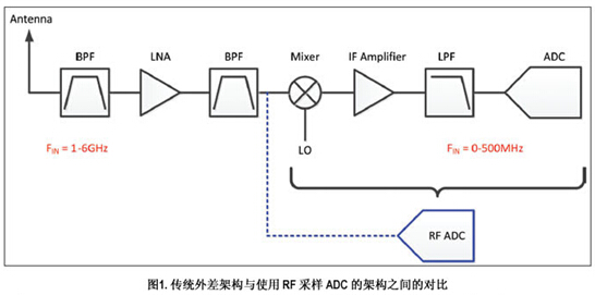
The RF sampling ADC directly acquires the RF input and thus replaces the entire downstream conversion stage shown in Figure 1. The use of an RF local oscillator (LO), mixer, and additional gain and filter stages saves printed circuit board (PCB) area and enables a more compact system design. The megahertz sampling clock of the ADC converts the sampled RF energy down to a lower digital intermediate frequency when the input is in the second Nyquist interval or higher, resulting in a high efficiency LO. Similar to the mixer LO in the heterodyne architecture, the ADC clock requires excellent phase noise to prevent energy from larger signals from mixing into the same frequency at which the small signal is located, as this reduces the sensitivity of the receiver.
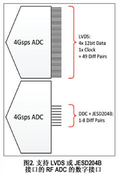
Traditional RF sampling ADCs require an extremely wide digital interface to output data. Since low-voltage differential signaling (LVDS) typically has a speed of only about 1 Gbps, a 12-bit, 4Gsps ADC would require approximately 49 differential pairs (48 of which are for data and the remaining one for clocks). This requires a sufficiently large package size and a large trace area on the PCB. For example, the ADC12J4000 uses a 10Gbps JESD204b interface that delivers the same amount of data with just eight differential pairs—reducing the number of differential pairs required by 83% (Figure 2). For narrowband applications, an on-chip digital decimation filter (DDC) enables on-chip chip filtering to further reduce data throughput and the number of channels required. For example, a signal with a bandwidth of 100 MHz can be transmitted at a rate of 250 Msps using only a single 5 Gbps channel (with a decimation factor of 32 for the IQ output).
The signal-to-noise ratio (SNR) of the RF sampling ADC is much lower than that of the IF sampling ADC, but the dynamic range does not deteriorate. The reason for this is that they use oversampling to compensate for the gap and achieve a similar SNR by normalizing the SNR per Hertz level.
For example, the signal-to-noise ratio is 14 bits for 70dB SNR, the noise spectral density (NSD) for a 250Msps ADC is -151dBFS/Hz, and the signal-to-noise ratio is 12 bits for 55dB SNR, and the NSD for a 4Gsps ADC is -148dBFS/Hz. The difference between them is only 3dB.
Advantages of RF sampling ADC
The RF sampling ADC has two distinct advantages. One is to digitize a large amount of signal bandwidth, and the other is to capture the signal directly on the RF, simplifying the signal chain.
But it also has the advantage that is rarely mentioned, that is, when the required signal band is much smaller than the sampling rate, it can use the fast sampling rate for frequency planning. Choosing a sample rate that is at least 5 to 10 times faster than the signal bandwidth allows the system designer to plan for the negative effects of in-band interferers that cannot be filtered out, thus enabling a better dynamic range.
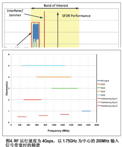
Similar to the heterodyne receiver, the spurious-free dynamic range (SFDR) performance of the ADC limits the detection of low input signals (Figure 3). The source of interference within the required bandwidth (or the interceptor in the communication infrastructure) cannot be filtered out. This requires the signal chain to reduce the gain to avoid ADC saturation. The reduced gain in the signal chain can impair the ability to boost small signals (eg, "useful signal B") above the ADC noise floor and thus cannot be properly detected. Harmonic spurs with in-band interferers also fall on top of the wanted signal, limiting the sensitivity of the receiver. This is a key element in military radars (used to detect small objects), software-defined radios and cellular base stations.
Using an RF sampling ADC (such as the ADC12J4000) in an oversampling configuration avoids the blocking of small, useful signals by the limiting harmonics of the interferer. For example, the required bandwidth of 200 MHz can be sampled at a sampling rate of 4 Gsps on an RF with a center frequency of 1.75 GHz. The first four are usually the worst harmonics in high-speed ADCs (HD2, HD3, HD4, and HD5), and other cross spurs from in-band interferers all fall outside the band (Figure 4).
The acceleration of the ADC sampling rate also relaxes the requirements for anti-aliasing filters required to drive amplifiers. The 200MHz band can be sampled with a 500Msps ADC, but a very accurate filter will be required because the next image is only 50MHz apart (assuming the band is at the center of the Nyquist zone). Conversely, the sampling rate is 4Gsps, and the same band centered at 1.75GHz requires only the same out-of-band filtering as the image with the closest distance of about 300MHz (alias = 2.15-2.35GHz, crossover image = 1150-1350MHz). The attenuation of the specifications and the requirements for the filter are much relaxed.
After successful use of frequency planning, SFDR performance is only limited by higher order harmonics (not any of HD2-5). These higher order spurs can be further improved by employing small signal jitter. The high sampling rate of the megasampled RF ADC provides a lot of "unoccupied" spectrum in which band-limited jitter can be placed without affecting any useful signals (Figure 5).
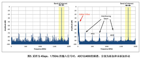
Jitter is a common technique in software-defined radios and can improve stray noise floor by 5 to 10 dB.
to sum up
Current RF sampling ADCs such as the ADC12J4000 can greatly improve the use and performance of ultra-wideband receivers. Its high input bandwidth directly realizes the digitization of the signal on the RF. At the same time, the fast sampling rate reduces the filter requirements and realizes the frequency planning around the harmonics of the in-band jammer. By adding on-chip digital filters to dramatically reduce digital interface data traffic, the ADC12J4000 is the perfect choice for small, low-power, next-generation digital radios.
Author: Tommy Neu, Texas Instruments (TI) Systems Engineer
Dongguan Jili Electronic Technology Co., Ltd. , https://www.jlglassoca.com