introduction
The Dual Tone Multi-Frequency (DTMF) signal was invented by Bell Labs and was originally used for user signaling between telephones and switches in a telephone system, typically for transmitting called numbers. The DTMF signal consists of a high frequency group and a low frequency group, and the high and low frequency groups each contain four frequencies. A high frequency signal and a low frequency signal are superimposed to form a combined signal representing a number. DTMF signaling has 16 codes. The dual tone multi-frequency dial keypad is a 4 x 4 matrix. Each time a button is pressed, a combination of high frequency and low frequency sinusoidal signals is sent. Since there is no harmonic interference between any two frequencies, the anti-interference ability is very strong, and the false positive rate after remote transmission is very low.
The DTMF and decoding chip in the switch uses CM8870 to realize the decoding function of the dual-tone multi-frequency signal on the communication line. The chip converts the detected dual-tone multi-frequency signal into a binary four-bit code and sends it to the single-chip microcomputer to provide data flow for the single-chip microcomputer. Purpose information. A dual tone multi-frequency signal is a group of combined signals composed of a high frequency signal and a low frequency signal. Dual-tone multi-frequency signal decoding is a very important part of the switch. Whether it can accurately decode the dual-tone multi-frequency signal sent by the line is the key to establish a communication link. Its working condition directly determines the reliability of remote data communication. Sex. The dual audio decoding chip CM8870 used in this system integrates a band separation filter and a digital decoder, which can convert the received DTMF signal into 8421 code.
1 CM8870 decoding function implementation
1.1 Introduction to CM8870 Chip CAMD's CM8870 dual-tone multi-frequency signal decoder is a single-chip 18-pin DIP package chip with filter and data decoding function to filter out non-audio signals from 340 to 3 400 Hz. At the same time, the audio signal is converted into a binary 4-bit digital signal, and the internal CMOS process greatly reduces the power consumption of the chip, and the power consumption is only 35 mW. The CM8870 includes a differential input amplifier, a clock generator and a tri-state latch interface bus, which reduces the peripheral components of the chip and requires only a normal crystal oscillator to operate normally. Its features are as follows: Provide DTMF signal separation filtering and decoding function; power consumption is less than 35 mW; can work in industrial temperature range; external crystal oscillator can be connected, and the oscillator contains the reference frequency signal; 18-pin DIP, EIAJ , OIC, PLCC package.
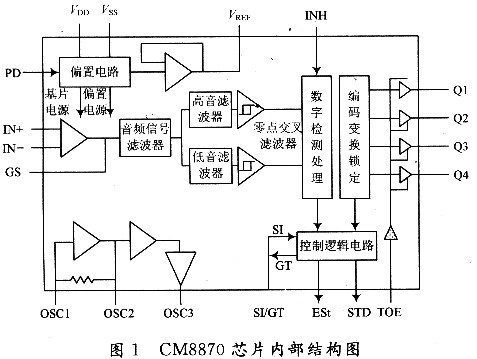
The basic feature of the CM8870 circuit is to provide DTMF signal separation filtering and decoding functions, and output a corresponding 4-bit parallel binary code of 16 DTMF frequency combinations. The binary code D1~D4 of the circuit output is controlled by the data output enable segment TOE. When TOE is high level, D1~D4 output the binary code corresponding to the currently input DTMF signal; when TOE is low level, D1~D4 end It is in a high resistance state. The op amp and R1, R2, and C1 form an inverting amplifier that isolates and amplifies the input DTMF signal with its gain. K=-R2/R1, change the value of R2 to change the gain. VREF is the reference voltage output, take VDD/2=2.5 V; INH and PD are internal circuit connection points, should be grounded; OSCl and OSC2 are Oscillator input and output, external 3.58 MHz crystal oscillator and internal oscillator generate reference frequency signal; STD is delay control output, output "1" when a set of valid dual audio signals are received, otherwise output "O"; ESt is the initial control output. If the circuit detects an identifiable tone pair, the terminal becomes high. If there is no input signal or continuous distortion, ESt returns to low level; SI/GT is the control input/ Time monitoring output. The functional block diagram is shown in Figure 1.
This article refers to the address: http://
A dual tone multi-frequency signal is a combination of two different frequency signals to represent a character or number. The two frequencies are selected from the low frequency band, one is selected from the high frequency band, and each frequency band contains four different frequencies, so that a total of 16 types can be combined, and only 12 kinds are commonly used, they are O~9, and #å· and *å·. The CM8870 can decode DTMF signals into 4-bit binary codes.
1.2 CM8870 receiving process CM8870 constitutes the receiving circuit, its input is from the analog user interface dual-tone multi-frequency signal, the output is 4-bit binary data for the processor to read from the data bus port. The process of receiving the number is as follows: after the analog signal is introduced from the IN pin, the out-of-band interference signal is initially filtered by the two-tone filter, and then the filtered signal is filtered out by the high group filter and the low group filter respectively. The high frequency and low frequency components are respectively sent to the digital detection calculation circuit after zero-crossing detection; the circuit further optimizes the audio signal to exclude external noise from being encoded by the encoder due to accidental inclusion of certain frequencies. Or affect the encoding of the encoder, causing subsequent harvest error. When the high and low frequency group signals are detected by the encoder at the same time, the ESt pin will output a high level as a flag for effectively detecting the DTMF signal, and when the DTMF signal disappears, the ESt pin will output a low level. In order to prevent external noise from being miscoded by the CM8870, the encoder requires that the encoded audio signal be maintained for a period of time, which is determined by an external RC circuit. As mentioned earlier, when the audio signal is detected, ESt outputs a high level of 1, the capacitor discharges, the voltage value on VC rises (assuming the signal exists internally throughout the required time), and when VC rises to a threshold value Vrst, The audio signal is encoded and becomes a digital signal that will be latched. At this point, GT is high, causing the voltage at the VC point to rise from the threshold to VDD. Thereafter, as long as ESt remains high GT is high, the external RC circuit returns to the initial state, and then, after a delay caused by a latch operation, the STD pin outputs a high level, indicating that the signal is latched. At this time, if you want to read the 4-bit code from Q1 to Q4, you should make TOE high and open the latch to complete the DTMF collection task.
2 single chip control CM8870 design
2.1 SM895l control block diagram SM8951 peripheral circuit connection As shown in Figure 2, the MCU is connected to the analog pick-up machine circuit through the P1.4 pin. When there is device call communication, the MCU will detect the off-hook action on the line through the pin. Then, the single-chip computer controls the ringing current generator to send a dial tone to the calling party. After receiving the number, the number is decoded by the DTMF and the decoder and sent to the single-chip microcomputer through the P2.7 pin, and the single-chip computer analyzes the number to determine the calling party. The object of the call, and then the MCU picks up the phone to determine whether the terminal switch is idle. If it is idle, it sends the call number. After receiving the response, it sends a ringing tone to the called party, and sends a ringback tone to the calling party. Then, the MCU immediately exits the operation and completes the call transfer.

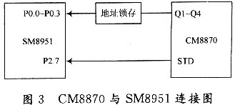
The interface circuit of CM8870 and SM8951 microcontroller is shown as in Fig. 3. PO of SM8951 microcontroller. O~PO. 3 Read the decoded data of CM8870. When CM8870 receives a valid DTMF signal, the ESt terminal first goes to the high level, and the SI level of the control input is raised by the integration circuit. If the SI terminal level is higher than the threshold. Level, the 4-bit binary code inside the CM8870 is updated, and the STD terminal goes high. The SM8951 microcontroller starts receiving after detecting this information through the P2.7 port. If the CM8870 has no DTMF signal input or DTMF signal continuous distortion, the ESt terminal is low level, the SI terminal is low level, and the STD terminal outputs low level.
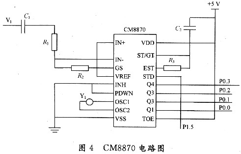
The dual audio decoding circuit is shown in Figure 4. The dual audio signal input point is connected to the collector V1 of a triode, and when V1 is turned on, the dual audio signal sent from the telephone line enters the CM8870. If the CM8870 receives a valid DTMF signal, it decodes the corresponding 8421 code and outputs it from the data output terminals Q1 to Q4. The data enters the single-chip PO. 0 to P0.3, complete data acquisition, judgment and processing. In addition, the status signal from the 15th pin of the CM8870 enters the P2.7 port of the microcontroller, and informs the microcontroller to read the data.
2.2 Single-chip microcomputer control process When the single-chip microcomputer controls the communication of the switch, it is necessary to monitor whether there is off-hook or hang-up action in the communication link. Off-hook and on-hook circuits are actually an electronic switch that controls the connection between the circuit board and the telephone line. Usually, this switch should be in the disconnected state to avoid causing the telephone line to be busy. When the remote control is needed, if the ringing sounds 5 times and no one answers, then the circuit board and the telephone line need to be connected. Machine action. V1 is an electronic switch, and the conduction of the switch is controlled by the P1.4 port of the MCU. If the circuit is off-hook, the circuit is simpler, but in practical use, it is found that the power consumption is large, and the 5 V relay pull-in current is as high as 30 μA, and the relay is also prone to spark interference. These problems are overcome by using a transistor off-hook circuit.
The software design flow chart is shown in Figure 5.
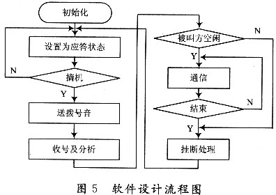
When the MCU controls the CM8870 as the calling party, the MCU must first initialize the CM8870, then control the off-hook circuit to pick up the phone. After receiving the dial tone of the called party, the MCU controls the ringing generator to generate ringing as the calling party. call. After waiting for a while, see if the other party has picked up the phone. If the other party picks up the phone, the communication starts, otherwise the phone hangs up and the communication ends.
When the relay is used as the called party, after starting the MCU, the program should first initialize the CM8870, and then detect whether there is a ringing tone at any time. If there is, the off-hook circuit of the MCU control picks up the machine actively, waits for a while, and ensures that it has been off-hook. After that, the MCU controls the ringer generator to generate a ringing as a calling party call. After waiting for a while, complete the call forwarding function, hang up, and end the communication.
3 Conclusion This system is based on SM8951 MCU and CM8870 dual-tone multi-frequency decoding chip to realize the function of small industrial control switch. This small switch can be used for remote data transmission of industrial control network with power line or twisted pair as transmission carrier, according to PSTN public telephone exchange network protocol and The signaling standard uses the circuit switching principle to implement the switching function. The small switch can be placed in a repeater of network communication or in a data processor at the end. Usually, the switch is only responsible for forwarding data, establishing a transmission link for data communication, and transmitting data in the switch in both directions. of. The switch is not the final destination of the data, but just a "station". Although with the development of digital communication technology, switching technology is becoming more and more complex, and switching functions are increasingly perfect, for industrial control networks, circuit-switched technology based on wired networks is still widely used for its low cost, easy implementation, high security and reliability. use.
Digital frame photo speaker:
Digital frame photo speaker is one type of dynamic speaker applications. we usually see many beautiful photo frame can play music, that is a new interesting point for the photo frame, it can bring us more beautiful memories along with the time we have these photo frame, . you can image you can hear the music and event the audio file when you look the photo frames, that sense is very good ~
Digital Photo Frame Speaker, Frame Speaker, Digital Frame Photos, Photos Frame Speaker
Shenzhen Xuanda Electronics Co., Ltd. , https://www.xdecspeaker.com