Many companies find that their electronic products are often dumped at the last level before they are sold on the shelves, which is in line with EMC requirements. This led them to recognize the importance of pre-testing and EMI diagnostics in the early design phase to minimize the impact of test failures – redesigns and equipment recalls, and delays in product launches. Wait until the end of the development period to understand whether the product can pass the conformance test is a gamble, because the development costs involved in each improvement will rise exponentially.
Therefore, it is increasingly important to troubleshoot EMI from design research, even after the prototype development, through trial production. Experimenting with the problem board and taking precautions can facilitate design.
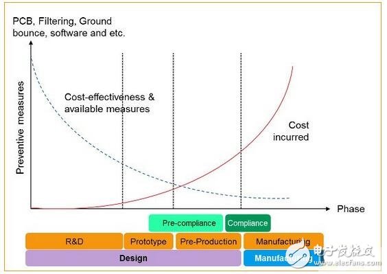
Figure 1: As the product progresses step by step during the development phase, the potential cost of the change increases, and the available measures to eliminate EMI problems are gradually limited.
Word: PCB, filtering, grounding, ground bounce, software, etc.; cost-effectiveness and available measures; preventive measures; cost of commitment; stage; pre-conformity test; conformance test; R&D; prototype; trial production; ;Production stage
Design engineers often find that new product designs require multiple modifications to reach the limits. They do not have EMI diagnostics, and EMI diagnosis is not part of their daily responsibility. Typically, the circuit board is designed to be submitted to the EMC department or external laboratory for further testing only when the designed circuit board is almost complete. However, making changes at this stage is challenging compared to the early design phase (some design considerations may be handled properly).
The results of the EMC compliance are design-controlled, capable of planning and the responsibility of the designer. Solving EMI is not about using witchcraft, nor does it require time domain engineers to avoid it. Using your familiar instrument, the oscilloscope, you can better understand EMI issues and understand the effects of the solution you are using.
Armed to do pre-conformity testingIn this regard, you might ask: So how do I use EMI filters and quasi-peak (QP) detectors? It depends on whether you are conducting a compliance test, a pre-compliance test, or doing an EMI troubleshooting. The EMI-type resolution bandwidth (RBW) filter is narrowband with a roll-off mode of 6dB instead of 3dB. The standard-compliant quasi-peak detector is based on the signal peak and repetition frequency to determine the weight from the peak.
Using incorrect filters and detectors can affect the amplitude and frequency values ​​returned by the device. In the conformance test, these two are mandatory standards. However, they are not decisive for EMI diagnosis because the primary purpose is to physically and electrically identify the source of radiation. If you don't have the actual consistency accuracy requirements, you get a close estimate that is sufficient.
If used to identify the source of radiation, it is sufficient to use a peak detector since the result of the quasi-peak detector algorithm is always less than or equal to the peak detector. Both the quasi-peak detector result and the peak detector result involve the same signal repetition rate, and you can formulate the math waveform or take this into account during the troubleshooting process. On the other hand, the EMI filter only slightly changes the result.
Unlike test receivers, oscilloscopes are not designed with built-in EMI compliance limits. Using the stencil test that most oscilloscopes have, or remote software, you can define EMI compliance limits on the oscilloscope to simulate EMI standard tests. You can then further set up more templates to find areas of interest.
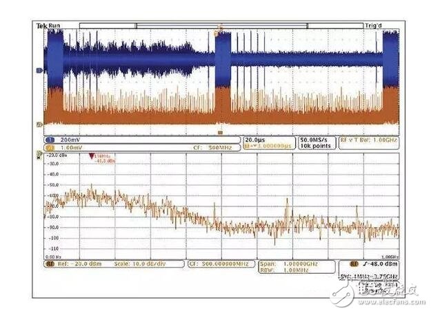
Figure 2: The limit line can be replaced with a template to determine if the device under test meets the requirements.
In the above figure, events that exceed the test limits can be further analyzed in the time domain. You can also set different RBWs in different frequency ranges on the oscilloscope.
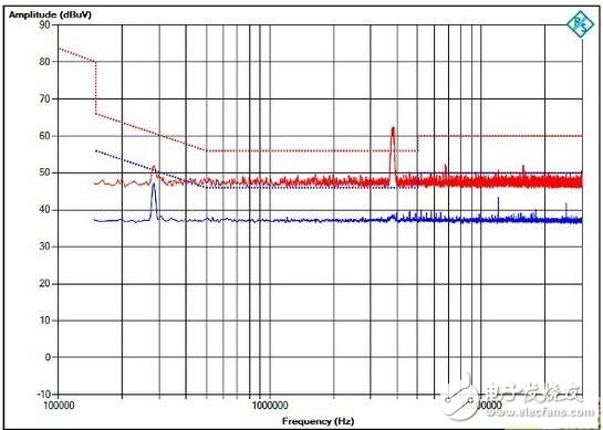
Figure 3: Test result output from RTO Scan software. RTO Scan is the EMI pre-test application for the R&S RTO Series oscilloscopes. The software provides a convenient comparison of the spectrogram output of logarithmic coordinates.
Figure word: amplitude, frequencyOscilloscopes are an effective tool for quickly understanding harmful emissions and finding their source. Accessing the time domain and frequency domain on the same instrument creates conditions for rapid analysis of harmful emissions. Because the oscilloscope is a commonly used instrument for hardware design engineers, it enhances the EMI troubleshooting capability during the development phase, and can perform the bottom test before going to the EMC lab, which significantly improves the success rate of the conformance test. The oscilloscope also provides you with a variety of techniques for locating, capturing, and analyzing radiation sources, which are summarized in the following table:
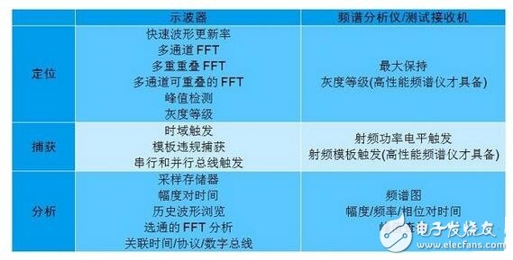
Table 1: A list of techniques for EMI diagnostics for oscilloscopes and traditional EMI test equipment, from positioning and capture to analyzing problematic sources of radiation.
EMI measurements require different methods than typical time domain related measurements or other common RF tests. In EMI, engineers never fully grasp what signals might exist. Since each new device under test is different, it is important to select the right tool and identify the source of the radiation based on the EMI signal characteristics.
When it comes to pre-compliance and compliance testing, the spectrum analysis capabilities of the oscilloscope are not a replacement for traditional EMI test equipment such as spectrum analyzers or test receivers. After all, the relatively limited dynamic range and bandwidth, the lack of preselectors, preamplifiers, and standard-compatible weighted detectors limit the use of oscilloscopes in EMI testing.
An oscilloscope, spectrum analyzer, or test receiver can solve EMI problems from different angles. Each device uses a different test method and offers different but complementary diagnostic techniques. The complementary approach of the oscilloscope opens up new horizons for EMI troubleshooting and provides unprecedented EMI troubleshooting capabilities. Combining existing analytic tools for EMI troubleshooting in your oscilloscope will help you quickly identify potential problems in your design.
What to do next? The power supply is the main source of EMI interference noise, and the power supply harmonic analysis of the oscilloscope has great potential in this type of troubleshooting. We will discuss this aspect soon. Four basic methods for troubleshooting EMI:Almost all governments around the world are trying to control the harmful electromagnetic interference (EMI) generated by electronic products produced in their country (see Figure 1). In order to provide users with a certain level of protection and security, the government will formulate very specific rules and regulations concerning the design of electronic products. Of course this is a good thing. But it also means that in order to minimize their EMI characteristics and pass official EMI certification testing, many companies must spend a lot of manpower and resources on product design and testing. The bad news is that even with good design principles, high quality components, and careful product characterization, EMI failures can still be affected if the test does not go well at all stages when performing compliance testing. Product release schedule.
Usually in order to avoid such a situation, the company will do some "pre-conformance" measurements during the design and prototype establishment phase. A better approach is to identify and fix potential EMI issues before the product is sent out for compliance testing.
Of course, most companies' laboratories do not have the test chamber conditions needed to make absolute EMI measurements. The good news is that it is completely feasible to identify and resolve EMI problems without copying test room conditions. Some of the techniques discussed in this article can help you reduce the risk of a product failing in the final complete EMC conformance assessment in the test room. This article also gives an example of determining signal characteristics and consistency in order to find an EMI source.
It is necessary to introduce the EMI test report before discussing the troubleshooting techniques. At first glance, the EMI report seems to provide information directly about the failure of a particular frequency point, so the thing seems simple: use the data in the report to determine which component in the design contains the source frequency of the problem, and pay special attention to it. A round of testing. However, while many of the test conditions are clearly stated in the report, some important things to consider may not be obvious. It is helpful to understand how the test room generates such reports when reviewing the design and trying to determine the source of the problem.
Look at the EMI test report shown in Figure 2, which shows a fault at about 90MHz.
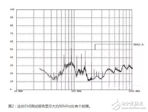
Figure 3 is a corresponding list data report detailing the test frequency, the measured amplitude, the corrected correction factor, and the adjusted field strength. Then compare the adjusted field strength with the indicator in the next column to determine the margin or excess amount, which is displayed in the rightmost column.
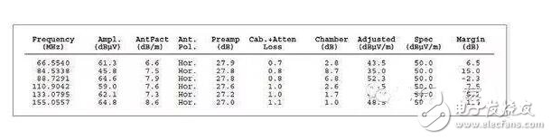
In the margin column shown in Figure 3, you can see that there is a peak that exceeds the limit specified by the specification at 88.7291 MHz, which is -2.3 compared to the specification.
Figure 3: This list of data corresponds to Figure 2, which shows that the fault point is at 88.7291 MHz, but there are many factors that make it doubtful whether this is the actual frequency.
You are done, are you? No, not so fast. Don't let all these numbers make you believe that this is the exact frequency of the problem EMI source. In fact, the frequency given in the test report is most likely not the actual source frequency. The International Committee on Radio Interference (CISPR) states that when performing radiation emission tests, different test methods must be used depending on the specific frequency range. Each range requires a filter and detector type for a particular resolution bandwidth, as shown in Table 1. The filter bandwidth determines the ability to resolve the actual frequency of interest; this means that the frequency range will vary in many ways to troubleshoot the source of the problem.
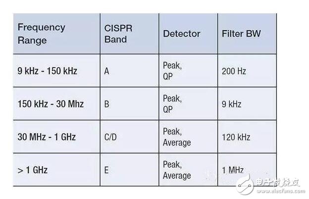
Table 1: CISPR test requirements vary according to different frequency ranges and affect frequency resolution.
It is important to note here that for certain frequency ranges, the CISPR test requires the use of a quasi-peak (QP) detector type that masks the actual frequency. Usually the EMI department or an external laboratory initially uses a simple peak detector to perform a scan to find the problem area. But when the signals found are above or near the specified limits, they also perform quasi-peak measurements. Quasi-peak is a method defined by the EMI measurement standard to detect the weighted peaks of the signal envelope. It weights the signal based on the duration and repetition rate of the signal to apply more weight to signals interpreted as "harassment" from a broadcast perspective. Higher frequency signals will result in higher quasi-peak measurements than non-frequent pulses. In other words, the more frequently the problem signal occurs, the more likely the absolute amplitude of the problem signal is blocked by the quasi-peak measurement.
The good news is that peak and quasi-peak scans are still useful for pre-conformance testing. Figure 4 shows an example of peak and quasi-peak detection. The figure shows a signal with a pulse width of 8 μs and a repetition rate of 10 ms, both in peak detection and quasi-peak detection. As a result, the quasi-peak detection result is 10.1 dB lower than the peak value.
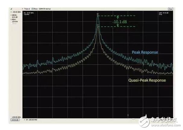
Figure 4: Comparison of peak detection and quasi-peak detection.
A good rule to remember is that the quasi-peak detection value is always less than or equal to the peak detection value and never greater than the peak detection value. So you can use peak detection to perform your EMI troubleshooting and diagnosis. You don't need to achieve the same level of accuracy as the EMI department or laboratory scans because the measurements are relative values. If the quasi-peak value in your lab report indicates that the design exceeds 3dB and the peak detection exceeds 6dB, then you know that the repair work you need is to reduce the signal by 3dB or more.
Scans from the test room for EMI reporting are usually performed under special conditions and may not be replicated by your company's laboratory. For example, the device under test (DUT) may be placed on a turntable to facilitate collecting signals from multiple angles. This azimuth information is useful because it indicates the DUT area where the problem occurs. Or the EMI test room may perform their measurements in a calibrated RF room and report the measurements as a strong field.
Fortunately, you don't need to completely copy the test room conditions to troubleshoot EMI tests. Unlike absolute measurements performed on highly controlled EMI test lines, the information in the test report can be used to gain insight into the measurement techniques used to generate the report and the relative observations around the device under test to isolate the source of the problem and estimate the effectiveness of the correction. To carry out troubleshooting work.
Where do you start to discover EMI radiation?It is time to focus our attention on harmful EMI sources. When we look at any product from an EMI perspective, the entire design can be seen as a collection of energy sources and antennas. Common (but not the only) sources of EMI problems include:
Power filterGround impedance
Not enough signal to return
LCD radiation
Component parasitics
Poor cable shielding
Switching power supply (DC/DC converter)
Internal coupling problem
Electrostatic discharge in a metal casing
Discontinuous return path
In order to determine the energy source on a particular board and the antenna at the center of a particular EMI problem, you need to check the period of the observed signal. What is the RF frequency of the signal? Is it pulsed or continuous? These signal characteristics can be monitored using a basic spectrum analyzer.
You also need to look at coincidence. Which signal on the device under test (DUT) coincides with the EMI event? It is common practice to use an oscilloscope to detect electrical signals on the DUT. Checking the coincidence of EMI and electrical events is undoubtedly the most time-consuming task in EMI troubleshooting. In the past, it has been difficult to correlate information from spectrum analyzers and oscilloscopes in a synchronized manner.
However, the introduction of a mixed-domain oscilloscope (MDO) has improved the situation by providing simultaneous and time-dependent observation and measurement functions. The instrument shown in Figure 5 can make it easy to see which signal coincides with which EMI event, which simplifies the EMI troubleshooting process.
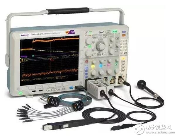
Figure 5: A mixed-domain oscilloscope (MDO) combines a spectrum analyzer, oscilloscope, and logic analyzer into a single meter to produce synchronized, time-correlated measurements from all three instruments. The picture shows the Tektronix MDO4000B.
MDO combines the functionality of a mixed-signal oscilloscope with the capabilities of a spectrum analyzer. With this combination, you can automatically display analog signal characteristics, digital timing, bus transactions, and RF and implement triggering based on this information. Some MDOs can also capture or observe spectrum and time domain trajectories, including RF amplitude versus time, RF phase versus time, and RF frequency versus time. The RF amplitude and time trajectory are shown in Figure 6.
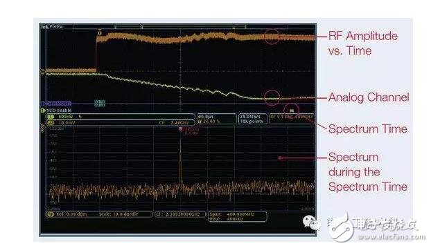
Figure 6: This figure shows the time-dependent observation function provided by MDO. The figure shows the trajectory of RF amplitude versus time.
Relative measurement with near field detectionAlthough the conformance test procedure is designed to produce an absolutely calibrated measurement, the troubleshooting effort can largely be performed using a relative measurement of the electromagnetic field occurring from the device under test. What's more, you can use MDO's spectrum analyzer function and RF channel to detect the wave resistance behavior in the near field to find the energy source. At the same time, you can probe the signal with a passive probe on one of the analog channels of the oscilloscope to discover the signal associated with the RF.
But first you have to know some background information about the electromagnetic field to be detected. Figure 7 shows the wave resistance behavior in the near and far fields and the transition between the two. As can be seen from the figure, in the near-field region, the field can range from the dominant magnetic field to the dominant electric field. In the near field, non-radiative behavior is dominant, so the wave resistance depends on the nature of the source and the distance from the source. In the far field, the impedance is fixed, and the measurement depends not only on the observed activity in the near field, but also on other factors such as antenna gain and test conditions.
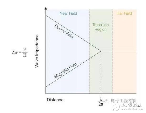
Figure 7: This figure shows the wave resistance behavior in the near and far fields and the transition between the two. Near field measurements can be used for EMI troubleshooting.
Near-field measurements are a measure that can be used for EMI troubleshooting because it does not require the test site to provide special conditions that allow you to identify the energy source. However, conformance testing is done in the far field, not near field. You usually don't use the far field because there are too many variables to make it complicated: the strength of the far-field signal depends not only on the strength of the source, but also on the radiation mechanism and the shielding or filtering measures that may be taken. As you should remember, if you can observe the signal in the far field, you should be able to see the same signal in the near field. (However, it is quite possible to observe the signal in the near field without seeing the same signal in the far field.) The near field probe is actually designed to pick up the magnetic field (H field) or the electric field (E field). antenna. In general, near field probes do not have calibration data, so they are suitable for relative measurements. If you are unfamiliar with the probes used to measure H-field and E-field variations, it is best to know some near-field probe designs and best practices:
The H-field (magnetic field) probe has a unique loop design as shown in Figure 8. What is important is that the direction of the H field probe is such that the loop plane is consistent with the conductor to be tested, such that the loop is arranged such that the flux line passes directly through the loop.
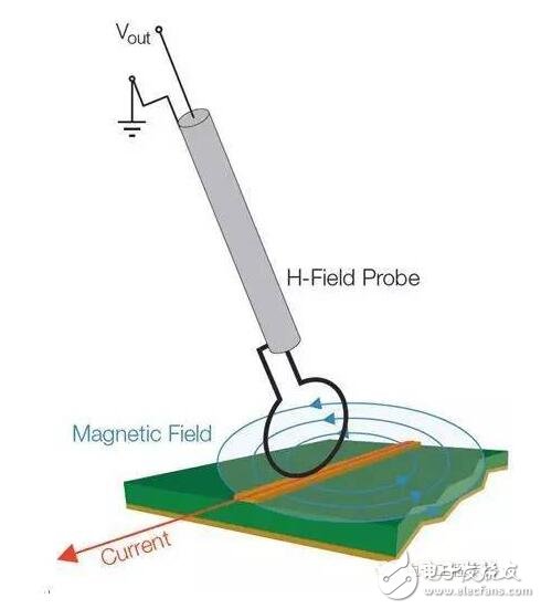
Figure 8: Aligning the H field probe with the current flow direction allows the magnetic field lines to pass directly through the loop.
The loop size determines the sensitivity and measurement area, so care must be taken when using this type of probe to isolate the energy source. Near field probe kits typically contain many different loop sizes so you can use a tapered loop size to reduce the measurement area.
H-field probes are very useful when identifying sources with relatively large currents, such as:
Low impedance node and circuit
Transmission line
power supply
Terminating wires and cables
The E-field (electric field) probe is used as a small monopole antenna and responds to changes in electric field or voltage. When using such probes, it is important that you keep the probe perpendicular to the measurement plane, as shown in Figure 9.
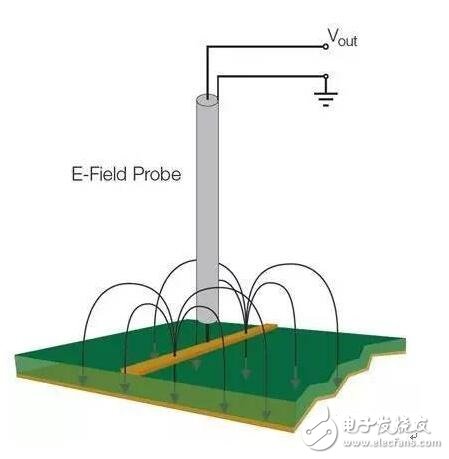
Figure 9: Place the E field probe perpendicular to the conductor to observe the electric field.
In practical applications, the E-field probe is best suited for finding very small areas and identifying sources with relatively high voltages and sources without terminations, such as:
High impedance nodes and circuits
Unterminated PCB trace
cable
At low frequencies, the impedance of the circuit nodes in the system can vary greatly; at this point a certain circuit or experimental knowledge is required to determine if the H field or E field can provide the highest sensitivity. At higher frequencies, these differences can be significant. In all cases, it is important to perform repetitive relative measurements so that you can be sure that the near-field radiation results due to any changes achieved can be accurately reproduced. Most importantly, the layout and aspects of the near-field probes should be consistent for each test change.
Tracking EMI radiation sourcesIn this example, the EMI scan of the small microcontroller indicates that there is an overrun fault that appears to be from a wideband signal with a center frequency of approximately 144 MHz. With the MDO's spectrum analyzer function, the first step is to connect the H field probe to the RF input and position the energy source with a relative near field measurement.
As mentioned above, it is important that the direction of the H field probe is such that the loop plane is consistent with the conductor to be tested. By moving the H field probe around the PCB, you can position the energy source. By selecting a probe that gradually reduces the aperture, you can position the search in a smaller area.
Once an apparent source of energy is located, the RF amplitude and time traces shown in Figure 10 can show the complete power versus time relationship for all signals in this range. Using this trace, you can clearly see that there is a large pulse in the display. Moving the spectrum time to pass the record length, it is obvious that the EMI event (the wideband signal centered at around 140 MHz) directly corresponds to this large pulse. To stabilize the measurement, turn on the RF power trigger and increase the record length to determine how often this RF pulse occurs. In order to measure the pulse repetition period, the measurement mark is turned on and the period is directly judged.
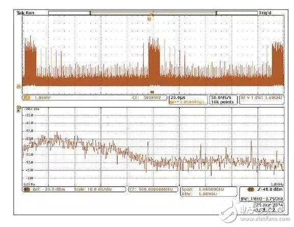
Figure 10: The RF amplitude and time trace of the MDO (above) shows a significant pulse at 140 MHz. The spectrum pattern (below) shows the frequency content of this pulse.
The next step in clearly determining the EMI source is to take advantage of the oscilloscope capabilities of MDO. With the same settings, turn on the analog channel 1 of the oscilloscope and browse the PCB to find the source that coincides with the EMI event.
After browsing the signal with the oscilloscope probe for a while, you can see the signal shown in Figure 11: in this case, a power filter. As you can clearly see from the display, the signal connected to channel 1 of the oscilloscope is directly related to the EMI event. It is now possible to develop an EMI repair plan to resolve this issue before conducting a certification test.

Figure 11: Using a passive probe on the oscilloscope analog channel to find the signal associated with the RF.
Summary of this articleFailure to pass EMI compliance testing may put product development plans at risk. However, pre-conformance testing can help you eliminate EMI problems before reaching this stage. Unlike absolute measurements in highly controlled EMI test lines, you can use the information in the EMI test report to make relative measurements and use it to isolate the source of the problem and estimate the repair effect.
Efficient EMI troubleshooting generally uses near-field detection methods to find relatively high electromagnetic fields, determine their characteristics, and then use a mixed-domain oscilloscope to correlate field activity with circuit activity to determine EMI sources. The troubleshooting techniques outlined in this article can effectively help you isolate harmful energy sources so that you can fix the problem before submitting it to EMI certification.
Antenk dip plug connector Insulation Displacement termination connectors are designed to quickly and effectively terminate Flat Cable in a wide variety of applications. The IDC termination style has migrated and been implemented into a wide range of connector styles because of its reliability and ease of use. Click on the appropriate sub section below depending on connector or application of choice.the pitch range from 1.27mm,2.0mm, and 2.54mm here.

IDC DIP Plug Connectors Key Specifications/Special Features:
Materials:
Insulator: PBT, glass reinforced, rated UL94V-0
Contact: phosphor bronze or brass
Electrical specifications:
Pitch: 1.27/2.0/2.54mm
Current rating: 1A, 250V AC
Contact resistance: 30M Ohms (maximum)
Insulation resistance: 3,000M Ohms, minute
Dielectric withstanding voltage: 500V AC for one minute
Operating temperature: -40 to +105 degrees Celsius
Terminated with 1.27mm pitch flat ribbon cable
Number of contacts: 06,08, 10, 12, 14, 16, 20, 24, 26, 30, 32,34, 40, 50, 60 and 64P
With RoHS mark
Used for ribbon cables
DIP Plug Connectors Application
Wire to Board
Apply to Industries : PC, IPC, Consumer Electronics, Automotive, Home Appliance, Medical
Dip Connector,Dip Plug Connector,Dip Direct Pulg Connector,IDC Plug Connector,Idc connector dip plug,1.27mm Dip Plug Connector,2.0mm Dip Plug Connector, and 2.54mm Dip Plug Connector
ShenZhen Antenk Electronics Co,Ltd , https://www.coincellholder.com