MEMS (Micro-Electro-Mechanical Systems) refers to mass-produced micro devices or systems that integrate micromachines, microactuators, signal processing and control circuits. MOEMS is the abbreviation of Micro-Opto-Electro- Mechanical System, which means micro-optical electromechanical system, which applies micro-optics to MEMS, which is an important application of MEMS in optical communication. A microphotoelectric mechanical chip generally refers to an optical system or an optoelectronic subsystem comprising more than one micromechanical component, and its application will cover various aspects such as optical communication, optical display, data storage, adaptive optics, and optical sensing.
With the rapid development of optical communication, the status of optical interconnection and optical switching as an optical network node is becoming more and more important. The optical switching device is a system component that realizes the on and off and cross connection of light with light as the core, and there is no photoelectric conversion. MEMS optical switches offer the advantages of low loss and high stability, independent of the data rate and signal protocol of the transmission. The practical MEMS optical switch principle is very simple, and its structure is essentially a two-dimensional microlens array. When performing optical exchange, the light is directly sent or reflected to different output ends of the optical switch by moving or changing the lens angle. MEMS optical switches use the principle of mechanical switches, but can be integrated on a single silicon substrate like a waveguide switch, thus combining the advantages of mechanical optical switches and waveguide optical switches, while overcoming their inherent shortcomings. MEMS optical switches have improved response speed and reliability, low insertion loss and crosstalk, low polarization and wavelength dependent losses, good adaptability to different environments, low power and control voltage, and latch-up.
2 MEMS optical switch control principle2.1 Introduction to MEMS Optical Switches
Typical MEMS optical switching devices can be divided into two-dimensional and three-dimensional structures. The spatially rotating mirror of the two-dimensional MEMS is monolithically integrated on the silicon substrate by surface micromachining techniques, and the collimated light is coupled to the appropriate output by appropriate rotation of the micromirror. The micro-hinge hinges the micro-mirror on the silicon substrate. There are two push rods on both sides of the micro-mirror. One end of the push rod is connected to the micro-mirror hinge point, and the other end is connected to the translatable dressing electrode. The switching state causes the micromirror to rotate by adjusting the dressing electrode. When the micromirror is horizontal, the beam can be passed over the micromirror. When the micromirror is rotated perpendicular to the silicon substrate, it will reflect the beam incident on its surface. Thereby the beam is output from the corresponding output port of the micromirror. The mirror of a three-dimensional MEMS can be deflected in any direction. These arrays usually appear in pairs. The input light reaches the mirror surface of the first array and is reflected onto the mirror of the second array, and the light is reflected to the output port.
Among various possible driving methods, electrostatic and magnetic induction methods are the main options. Electrostatic methods rely on mutual attraction between mechanical elements of opposite charge polarity, which is the main driving method used in MEMS technology, and it has the advantages of repeatability and easy shielding. Magnetic induction drive relies on mutual attraction between magnets or electromagnets. Although the magnetic induction drive can generate more driving force and has higher linearity, since there are still many problems to be solved in the magnetic induction application, the current electrostatic driving scheme is still the best choice for reliable equipment.
The control scheme described in this paper is aimed at a two-dimensional structure, a MEMS optical switch driven by an electrostatic method.
2.2 Control Principles and Processes
The MEMS 4&TImes;4 optical switch is one of the core subsystems in the OXC node device. It is responsible for routing the four wavelengths of light as required in the whole system to achieve the purpose of optical switching.
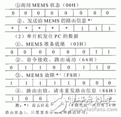
The advantage of the MEMS optical switch is that the switching of the optical wave routing is accomplished by external control information and corresponding high and low level control of the internal 16 microlenses uplift or not. The MEMS optical switch we choose is specified in the format of the control information. No matter how many microlenses are inside, it needs to be controlled by a series of 64-bit serial data consisting of "1" and "0".
Depending on the specific operating principle of the MEMS optical switch and the timing relationship between the desired digital signals, the required 64-bit control information, as well as other signals (such as CLK, ENA signals), can be provided by a high speed microcontroller.
During the debugging of the board, the control system simulates the local control by the corresponding program of a PC, and sends corresponding routing information. The information of the PC is sent to the MCU through the serial port, and the MCU performs further control actions. The information such as the success or failure of the MEMS optical switch is read by the microcontroller to read the 64-bit control data in its internal register, which is compared with the original correct 64-bit data. After the operation is completed, the MCU generates corresponding feedback information to the PC through the serial port. Form the interaction between man-machine, remote and local.
In order to maintain compatibility with the entire OXC system, the MEMS subsystem can be controlled directly from the FPGA chip in a dedicated main control circuit, in addition to being controlled by a local microcontroller. In this way, you can ensure that the subsystem is safe. To this end, the circuit design will also retain an interface for it.
3 control system designBased on the foregoing principles, the design of the subsystem will be divided into two aspects of hardware and software design.
3.1 Hardware design
The test phase will design four control channels for the MEMS, which retain the manufacturer's test board circuit and use it as a control channel; provide two channels for different types of control information of the local microcontroller; in addition, control the FPGA chip that may be used in the future The information is reserved for one channel. In the actual application phase, only one MCU channel and one FPGA control channel will be reserved.
During the debugging of the board, the routing and management information comes from the PC software of the analog network management. In practical applications, all routing and management information will be autonomously controlled in the future. Figure 1 is a block diagram of the hardware design.
Although there are more than one control channel in the experimental and practical phases, there is only one channel that works during a certain period. The switching of the channel is done by manual jumper.
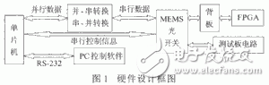
The single-chip microcomputer selects the single-chip microcomputer with high speed and low consumption dual serial port and multiple interrupts. This microcontroller will provide 64-bit control information and other control signals required for the MEMS optical switch, such as the clock CLK signal, routing enable signal, and so on.
The parallel-serial conversion circuit is used to convert the control information sent by the single-chip microcomputer into serial data required by the MEMS. This function is jointly performed by the MCU and the parallel-serial conversion chip; the serial-to-parallel conversion circuit is used for parallel reading of the serial original routing information in the MEMS internal register by the MCU. This function is performed by a single chip and a serial-to-parallel conversion chip.
3.2 Software design plan:
Because human-computer interaction is required in debugging, a set of PC programs and microcontroller control programs are required. Two sets of programs communicate via the RS-232 interface. The communication protocol between programs is formulated as follows:
(1) Data sent by the PC to the microcontroller
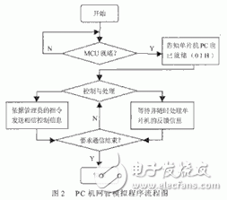
The PC program uses a graphical interface, and various information sent and received will give the administrator a real-time prompt on the program interface. Figure 2 shows the flow chart of the PC network management simulation program.
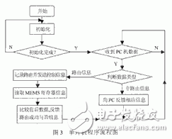
Compared with the PC program, the single-chip microcomputer control program has difficulty in transmitting the clock signal, the enable signal, and the like required by the MEMS, and transmitting the 64-bit microlens control data. There is a strict timing relationship between these signals. Special attention should be paid to the delay program and instruction writing skills when programming. The program flow chart of the single chip microcomputer is shown in Figure 3.
Through the coordination of software and hardware, the MEMS optical switch subsystem can smoothly complete the arbitrary switching of multiple optical wave routes. During the debugging phase, the administrator uses the computer software to simulate the network management to send routing control commands to the MCU on the MEMS control board. In actual applications, this routing control command is issued by the main control board in the system. After receiving the instruction, the MCU issues a specific instruction that meets the MEMS optical switch control requirements, and controls the corresponding action of the internal lens of the MEMS optical switch, thereby completing the cross connection of the optical path. This process does not require any optical-to-electrical conversion.
What are the advantages of Explosion-proof Screen Protectors?
What is an Explosion-proof Screen Protector? This is a Soft Film made of imported PET material. It has very good flexibility and can help you solve the problems of tilting, white edges, and not suitable for curved screens. Can closely fit the curved edge of the screen.
The PET Screen Protector is made of imported materials from Korea. It is equipped with a proprietary "self-healing" function that can automatically repair minor scratches on the film. Daily protection measures to prevent accidental knocks and drops. The screen strengthens the screen and reduces the chance of cracking. Broken tempered glass is no longer replaced frequently.
1. Edge coverage: The Explosion-proof Screen Protective Film is made of PET flexible material, which is very suitable for the screen of your device, and 100% provides excellent edge coverage, and there is no gap between the edges of the device
2. High-definition resolution: high-definition display, true display of the original screen color.
3. Original touch experience: The oleophobic coating surface of the screen protector can provide your phone with original texture and perfect touch screen response speed. The Soft Film also has oleophobicity and water resistance, which can prevent unnecessary fingerprints.
4. Self-repairing scratches: The Screen Protection Film with self-repairing function can automatically repair tiny scratches and bubbles within 24 hours.
5. Anti-seismic and explosion-proof: PET material has high strength, flexibility and elasticity, which can fully decompose the impact force and prevent the mobile phone from breaking
Explosion-Proof Matte Protective Film,Matte Explosion-Proof Screen Protector,Anti-Scratch Matte Film,Anti-Impact Matte Film
Shenzhen TUOLI Electronic Technology Co., Ltd. , https://www.hydrogelprotectors.com