OverviewThis applicaTIon note discusses how to connect the DS31256 to the DS2155, DS21Q55, and DS21Q50 in T1 / E1, 2MHz, 4MHz, 8MHz clock mode. The hardware connection and software configuration details are given.
Dallas Semiconductor offers a complete line of communications products. The devices provide highly integrated solutions for applications including T-carrier and E-carrier, broadband, and so on.
The DS31256 has 256 independent directional HDLC channels and supports up to 64 T1 or E1 data streams simultaneously. It supports 16 channelized or unchannelized ports and each channelized port can handle one, two or four T1 or E1 lines. There are also three fast ports on the that can each handle up to 52Mbps in both transmit and receive directions, suitable for VDSL, HSSI, or clear-channel T3 applications. All 16 ports can operate from 0 to 10Mbps when configured in unchannelized mode, and gapped clocking is supported on all ports.
The DS2155 and DS21Q55 enable the user to select-under software control-T1, E1, or J1 protocol. This simplifies the design of low-cost multiprotocol interfaces. A high-performance LIU, flexible architecture, and rich feature set make the DS2155 an excellent solution to all standard T1, E1, and J1 applications including routers, switches, muxes, ADMs, and CSU / DSUs.
The DS21Q50 contains all functions necessary for connecting to four E1 lines. It is ideally suitable for E1 data pipe applications where high performance must be achieved at a low price. In addition to the four transceivers, an extra jitter attenuator resource is available to clean up transmit or backplane clocks. A clock synthesizer is available for generating backplane clocks from 2.048MHz to 16.384MHz and a single clock synthesizer can be shared between multiple DS21Q50s to facilitate smooth clock-source switching.
1 Connection with DS2155 1.1 Connection in T1 Mode Hardware Configuration Figure 1 shows the connection between DS2155 and DS31256 in T1 mode. The receive elastic store is bypassed in the framer because the transmit clock is sourced from the RCLK pin. The transmit synchronization signal is sourced from the RSYNC pin.
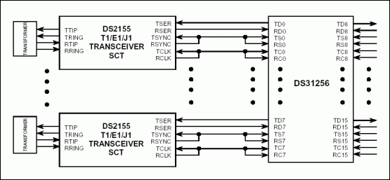
Figure 1. DS2155 connected to DS31256 in T1 and E1 mode.
Software ConfigurationTables 1 and 2 show some of the critical register settings necessary to initialize the DS31256 and DS2155 for the operation described above. Note that they might not represent the complete register listing required for a customer application. The reader is encouraged to refer to device data sheets for further information regarding the flexibility of the DS31256 and DS2155.
Table 1. Register setting for DS31256 in T1 mode
| SETTING | LOCATION | FUNCTION |
| RSSO = 0 RSS1 = 0 RUEN = 0 | RP [n] CR | Set Rx port T1 mode; Set Rx port channelized mode enable |
| TSSO = 0 TSS1 = 0 TUEN = 0 | TP [n] CR | Set Tx port T1 mode; Set Tx port channelized mode enable |
Table 2. Register settings for DS2155 in T1 mode
| SETTING | LOCATION | FUNCTION |
| T1 / E1 = 0 | MSTRREG.1 | Select the T1 operating mode |
| TSIO = 0 RSIO = 0 | IOCR1.1 IOCR1.4 | TSYNC is an output RSYNC in an output |
| TCLKINV = 0 RCLKINV = 0 | IOCR2.6 IUOCR2.7 | TCLK no inversion RCLK no inversion |
| RB8ZS = 1 RFM = 1 | T1RCR2.5 T1RCR2.6 | Receive B8ZS enabled Receive ESF framing mode |
| TB8ZS = 1 | T1TCR2.7 | Transmit B8ZS enabled |
| TFM = 1 | T1CCR1.2 | Transmit ESF framing mode |
| RESE = 0 | ESCR.0 | Receieve elastic store is bypassed |
| TPD = 1 | LIC1.0 | Normal transmitter operation |
| TUA = 1 ETS = 0 | LIC2.4 LIC2.7 | Transmit data normally T1 mode selected |
Software ConfigurationTables 3 and 4 show some of the critical register settings necessary to initialize the DS31256 and DS2155 for operation as described above. Note that they might not represent the complete register listing required for a customer application. The reader is encouraged to refer to the device data sheet for further information regarding the flexibility of the DS31256 and DS2155.
Table 3. Register setting for DS31256 in E1 mode
| SETTING | LOCATION | FUNCTION |
| RSSO = 0 RSS1 = 1 RUEN = 0 | RP [n] CR | Set Rx port E1 mode; Set Rx port channelized mode enable |
| TSSO = 0 TSS1 = 1 TUEN = 0 | TP [n] CR | Set Tx port E1 mode; Set Tx port channelized mode enable |
Table 4. Register settings for DS2155 in E1 mode
| SETTING | LOCATION | FUNCTION |
| T1 / E1 = 1 | MSTRREG.1 | Select the E1 operating mode |
| TSIO = 0 RSIO = 0 | IOCR1.1 IOCR1.4 | TSYNC is an output RSYNC in an output |
| TCLKINV = 0 RCLKINV = 0 | IOCR2.6 IUOCR2.7 | TCLK no inversion RCLK no inversion |
| SYNCE = 0 RHDB3 = 1 RSIGM = 1 | E1RCR1.1 E1RCR1.5 E1RCR1.6 | Receive auto resync enabled Receive HDB3 enabled Receive CCS signaling mode |
| RCRC4 = 1 | E1RCR1.3 | Receive CRC4 enabled |
| TCRC4 = 1 THDB3 = 1 | E1TCR1.0 E1TCR1.2 | Transmit CRC4 enabled Transmit HDB3 enabled |
| RESE = 0 | ESCR.0 | Receieve elastic store is bypassed |
| TPD = 1 | LIC1.0 | Normal transmitter operation |
| TUA = 1 ETS = 1 | LIC2.4 LIC2.7 | Transmit data normally E1 mode selected |
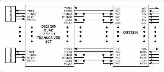
Figure 2. DS21Q55 connected to DS31256 in T1 mode.
Software ConfigurationTables 5 and 6 show some of the critical register settings necessary to initialize the DS31256 and DS21Q55 for operation as described above. Note that they might not represent the complete register listing required for a customer application. The reader is encouraged to refer to the device data sheet for further information regarding the flexibility of the DS31256 and DS21Q55.
Table 5. Register setting for DS31256 in T1 mode
| SETTING | LOCATION | FUNCTION |
| RSSO = 0 RSS1 = 0 RUEN = 0 | RP [n] CR | Set Rx port T1 mode; Set Rx port channelized mode enable |
| TSSO = 0 TSS1 = 0 TUEN = 0 | TP [n] CR | Set Tx port T1 mode; Set Tx port channelized mode enable |
Table 6. Register settings for DS2155 in T1 mode
The following settings apply to all four ports (transceivers):
| SETTING | LOCATION | FUNCTION |
| T1 / E1 = 0 | MSTRREG.1 | Select the T1 operating mode |
| TSIO = 0 RSIO = 0 | IOCR1.1 IOCR1.4 | TSYNC is an output RSYNC in an output |
| TCLKINV = 0 RCLKINV = 0 | IOCR2.6 IUOCR2.7 | TCLK no inversion RCLK no inversion |
| RB8ZS = 1 RFM = 1 | T1RCR2.5 T1RCR2.6 | Receive B8ZS enabled Receive ESF framing mode |
| TB8ZS = 1 | T1TCR2.7 | Transmit B8ZS enabled |
| TFM = 1 | T1CCR1.2 | Transmit ESF framing mode |
| RESE = 0 | ESCR.0 | Receieve elastic store is bypassed |
| TPD = 1 | LIC1.0 | Normal transmitter operation |
| TUA = 1 ETS = 0 | LIC2.4 LIC2.7 | Transmit data normally T1 mode selected |
2.2 Connection in 8M Mode Hardware Configuration Figure 3 shows the connection between DS21Q55 and DS31256 in 8M mode. The four E1 data bus on the backplane bus is in frame interleave mode. The receive elastic store is enabled. The transmit clock is source from RCLK pin. The 8kHz transmit synchronization signal is generated from the RSYNC pin of the first device on the bus. All other devices on the bus have their frame syncs configured as inputs.
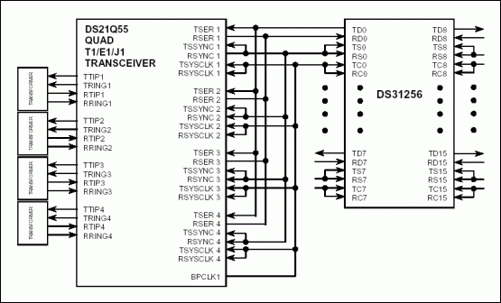
Figure 3. DS21Q50 connected to DS31256 in 8M mode.
Software ConfigurationTables 7 and 8 show some of the critical register settings necessary to initialize the DS31256 and DS2155 for operation as described above. Note that they might not represent the complete register listing required for a customer application. The reader is encouraged to refer to the device data sheet for further information regarding the flexibility of the DS31256 and DS2155.
Table 7. Register setting for DS31256 in 8M mode
| SETTING | LOCATION | FUNCTION |
| RSSO = 1 RSS1 = 1 RUEN = 0 | RP [n] CR | Set Rx port 8.192MHz mode; Set Rx port channelized mode enable |
| TSSO = 1 TSS1 = 1 TUEN = 0 | TP [n] CR | Set Tx port 8.192MHz mode; Set Tx port channelized mode enable |
Table 8. Register settings for DS2155 in 8M mode
The following settings apply to all four ports (transceivers):
| SETTING | LOCATION | FUNCTION |
| T1 / E1 = 1 | MSTRREG.1 | Select the E1 operating mode |
| TCLKINV = 0 RCLKINV = 0 | IOCR2.6 IUOCR2.7 | TCLK no inversion RCLK no inversion |
| SYNCE = 0 RHDB3 = 1 RSIGM = 1 | E1RCR1.1 E1RCR1.5 E1RCR1.6 | Receive auto resync enabled Receive HDB3 enabled Receive CCS signaling mode |
| RCRC4 = 1 | E1RCR1.3 | Receive CRC4 enabled |
| TCRC4 = 1 THDB3 = 1 | E1TCR1.0 E1TCR1.2 | Transmit CRC4 enabled Transmit HDB3 enabled |
| RESE = 0 | ESCR.0 | Receieve elastic store is bypassed |
| TPD = 1 | LIC1.0 | Normal transmitter operation |
| TUA = 1 ETS = 1 | LIC2.4 LIC2.7 | Transmit data normally E1 mode selected |
| RSCLKM = 1 TSCLKM = 1 | IOCR2_S1.0 IOCR2_S1.1 | IBO enabled IBO enabled |
The following settings apply to the specified port (transceiver):
| BPEN = 1 BPCS0 = 1 BPCS1 = 0 | TC # 1, CCR2.0 TC # 1, CCR2.1 TC # 1, CCR2.2 | Enable BPCLK1 pin Backplane clock select 8.192MHz |
| TSIO = 0 RSIO = 0 | TC # 1, IOCR1.1 TC # 1, IOCR1.4 | TSYNC is an input RSYNC is an output |
| TSIO = 0 RSIO = 1 | TC # 2, IOCR1.1 TC # 2, IOCR1.4 | TSYNC2 is an input RSYNC2 is an input |
| TSIO = 0 RSIO = 1 | TC # 3, IOCR1.1 TC # 3, IOCR1.4 | TSYNC3 is an input RSYNC3 is an input |
| TSIO = 0 RSIO = 1 | TC # 4, IOCR1.1 TC # 4, IOCR1.4 | TSYNC4 is an input RSYNC4 is an input |
| DA0 = 0 DA1 = 0 DA2 = 0 IBOEN = 1 IBOSEL = 1 IBS0 = 1 IBS1 = 0 | TC # 1, IBOC.0 TC # 1, IBOC.1 TC # 1, IBOC.2 TC # 1, IBOC.3 TC # 1, IBOC.4 TC # 1, IBOC.5 TC # 1, IBOC.6 | This is Transceiver # 1 on the bus. Interleave Bus Operation enabled Frame Interleave Operation Four transceivers on the bus |
| DA0 = 1 DA1 = 0 DA2 = 0 IBOEN = 1 IBOSEL = 1 IBS0 = 1 IBS1 = 0 | TC # 1, IBOC.0 TC # 1, IBOC.1 TC # 1, IBOC.2 TC # 1, IBOC.3 TC # 1, IBOC.4 TC # 1, IBOC.5 TC # 1, IBOC.6 | This is Transceiver # 2 on the bus. Interleave Bus Operation enabled Frame Interleave Operation Four transceivers on the bus |
| DA0 = 0 DA1 = 1 DA2 = 0 IBOEN = 1 IBOSEL = 1 IBS0 = 1 IBS1 = 0 | TC # 1, IBOC.0 TC # 1, IBOC.1 TC # 1, IBOC.2 TC # 1, IBOC.3 TC # 1, IBOC.4 TC # 1, IBOC.5 TC # 1, IBOC.6 | This is Transceiver # 3 on the bus. Interleave Bus Operation enabled Frame Interleave Operation Four transceivers on the bus |
| DA0 = 1 DA1 = 1 DA2 = 0 IBOEN = 1 IBOSEL = 1 IBS0 = 1 IBS1 = 0 | TC # 1, IBOC.0 TC # 1, IBOC.1 TC # 1, IBOC.2 TC # 1, IBOC.3 TC # 1, IBOC.4 TC # 1, IBOC.5 TC # 1, IBOC.6 | This is Transceiver # 4 on the bus. Interleave Bus Operation enabled Frame Interleave Operation Four transceivers on the bus |
Where:
TC # 1 = Transceiver # 1 (TS1, TS0 = 00)
TC # 2 = Transceiver # 2 (TS1, TS0 = 01)
TC # 3 = Transceiver # 3 (TS1, TS0 = 10)
TC # 4 = Transceiver # 4 (TS1, TS0 = 11)
3 Connection with DS21Q50 3.1 Connection in 2M Mode Hardware Configuration Figure 4 shows the connection between the DS21Q50 and DS31256 in 2M mode. As the IBO function is disabled, the transmit clock of each port is source from TCLK pin, which is connected to SYSTLK1. The Layer 1 of DS31256 is configured as E1 port.
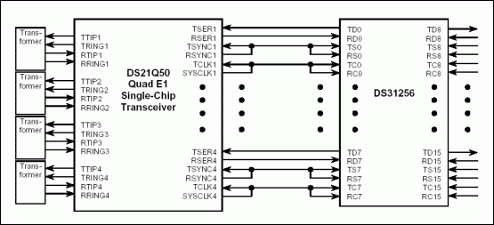
Figure 4. DS21Q50 connected to DS31256 in 2M mode.
Software ConfigurationTables 9 and 10 show some of the critical register settings necessary to initialize the DS31256 and DS21Q50 for operation as described above. Note that they might not represent the complete register listing required for a customer application. The reader is encouraged to refer to the device data sheet for further information regarding the flexibility of the DS31256 and DS21Q50.
Table 9. Register setting for DS31256
| SETTING | LOCATION | FUNCTION |
| RSSO = 0 RSS1 = 1 RUEN = 0 | RP [n] CR | Set Rx port E1 mode; Set Rx port channelized mode enable |
| TSSO = 0 TSS1 = 1 TUEN = 0 | TP [n] CR | Set Tx port E1 mode; Set Tx port channelized mode enable |
Table 10. Register settings for DS21Q50
The following settings apply to all four ports (transceivers):
| SETTING | LOCATION | FUNCTION |
| IBOEN = 0 | IBO.3 | Disable IBO operation |
| RSIO = 0 | RCR.5 | RSYNC pin is an output |
| RSM = 0 | RCR.6 | RSYNC is in frame mode |
| TSIO = 0 | TCR.0 | TSYNC in an input |
| TSM = 0 | TCR.1 | TSYNC is in frame mode |
3.2 Connection in 8M Mode Hardware Configuration Figure 5 shows the connection between the DS21Q50 and DS31256 in 8M mode. In order to ensure data integrity in IBO mode, all clock and sync signals should be phase-aligned. The receive-elastic store for each of the four transceivers must be enabled. They should all receive the same frame-reference pulse (RSYNC) and 8.192MHz system clock (SYSCLK). In this case, the phase-locked frame pulse is provided by the system backplane; and the 21Q50's system- clock synthesizer provides the 8.192MHz clock. Note that the 8.192MHz clock can be created internally from any of the four E1 line recovered clocks. In IBO mode, the DS21Q50 can create transmit clock (TCLK) for each E1 formatter by dividing down the applied SYSCLK. The Layer 1 of DS31256 is configured as channelized 8MHz port.
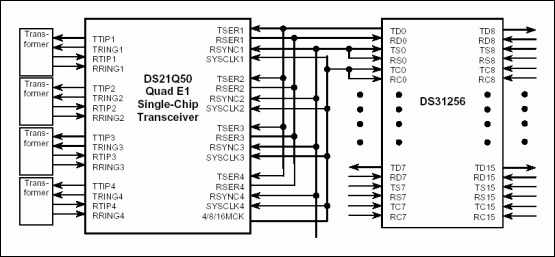
Figure 5. DS21Q50 connected to DS31256 in 8M mode.
Software ConfigurationTables 11 and 12 show some of the critical register settings necessary to initialize the DS31256 and DS21Q50 for operation as described above. Note that they might not represent the complete register listing required for a customer application. The reader is encouraged to refer to the device data sheet for further information regarding the flexibility of the DS31256 and DS21Q50.
Table 11. Register settings for DS31256
The following settings apply to all four ports (transceivers):
| RSSO = 1 RSS1 = 1 RUEN = 0 | RP [n] CR | Set Rx port 8.192MHz mode; Set Rx port channelized mode enable |
| TSSO = ` TSS1 = 1 TUEN = 0 | TP [n] CR | Set Tx port 8.192MHz mode; Set Tx port channelized mode enable |
Table 12. Register settings for DS21Q50
The following settings apply to all four ports (transceivers):
| SETTING | LOCATION | FUNCTION |
| IBOEN = 1 | IBO.2 | Enable IBO operation |
| IBOTCS = 1 | IBO.6 | Transmit clock derived from SYSCLK |
| SCS0 = 0 SCS1 = 1 | IBO.4 IBO.5 | 8.192MHz operation (4 ports on the PCM bus) |
| RESE = 1 | RCR.4 | Enable receive elastic store |
| RSIO = 1 | RCR.5 | RSYNC pin is an input |
| RSM = 0 | RCR.6 | RSYNC is in frame mode |
| TSIO = 1 | TCR.0 | TSYNC in an output |
| TSM = 0 | TCR.1 | TSYNC is in frame mode |
The following settings apply to the specified port (transceiver):
| SCS0 = 1 SCS1 = 0 SCS2 = 0 | TC # 1, SCICR.0 TC # 1, SCICR.1 TC # 1, SCICR.2 | Select the recovered clock from transceiver # 1 as the source for the system clock synthesizer |
| CSS0 = 0 CSS1 = 1 | TC # 1, SCICR.3 TC # 1, SCICR.4 | 8.192MHz operation (4 ports on the PCM bus) |
| SOE = 1 | TC # 1, SCICR.5 | Enable synthesizer clock output |
| DA0 = 0 DA1 = 0 DA2 = 0 | TC # 1, IBO.0 TC # 1, IBO.1 TC # 1, IBO.2 | Set transceiver # 1 as the first device on the PCM bus |
| DA0 = 1 DA1 = 0 DA2 = 0 | TC # 2, IBO.0 TC # 2, IBO.1 TC # 2, IBO.2 | Set transceiver # 2 as the second device on the PCM bus |
| DA0 = 0 DA1 = 1 DA2 = 0 | TC # 3, IBO.0 TC # 3, IBO.1 TC # 3, IBO.2 | Set transceiver # 1 as the third device on the PCM bus |
| DA0 = 1 DA1 = 1 DA2 = 0 | TC # 4, IBO.0 TC # 4, IBO.1 TC # 4, IBO.2 | Set transceiver # 4 as the fourth device on the PCM bus |
| TSM = 0 | TCR.1 | TSYNC is in frame mode |
Where:
TC # 1 = Transceiver # 1 (TS1, TS0 = 00)
TC # 2 = Transceiver # 2 (TS1, TS0 = 01)
TC # 3 = Transceiver # 3 (TS1, TS0 = 10)
TC # 4 = Transceiver # 4 (TS1, TS0 = 11)
4 Connection with DS26528 4.1 Connection in 8M Mode Hardware Configuration Figure 6 shows the connection between DS26528 and DS31256 in 8M mode. Two four E1 data bus (A and B) on the backplane bus is in frame interleave mode. The receive elastic store is enabled. The transmit clock is source from RCLK pin. The 8kHz transmit synchronization signal is generated from the RSYNC pin of the first device on the bus. All other devices on the bus have their frame syncs configured as inputs.
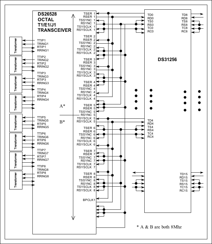
Figure 6. DS26528 connected to DS31256 in 8M mode.
Software ConfigurationTables 13 and 14 show some of the critical register settings necessary to initialize the DS31256 and DS26528 for operation as described above. Note that they might not represent the complete register listing required for a customer application. The reader is encouraged to refer to the device data sheet for further information regarding the flexibility of the DS31256 and DS26528.
Table 13. Register Settings for DS31256 in 8M Mode
| SETTING | LOCATION | FUNCTION |
| RSS0 = 1 RSS1 = 1 RUEN = 0 | RP [n] CR | Set Rx port 8.192MHz mode; set Rx port channelized mode enable |
| TSS0 = 1 TSS1 = 1 TUEN = 0 | TP [n] CR | Set Tx port 8.192MHz mode; set Tx port channelized mode enable |
Table 14. Register Settings for DS26528 in 8M Mode
The following settings apply to all 8 ports (transceivers):
| SETTING | LOCATION | FUNCTION |
| T1 / E1 = 1 | TMMR.0 & RMMR.0 | Select the E1 operating mode |
| FRM_EN = 1 | TMMR.7 & RMMR.7 | Framer enabled |
| TCLKINV = 0 RCLKINV = 0 | TIOCR.7 RIOCR.7 | TCLK no inversion RCLK no inversion |
| SYNCE = 0 | RCR1.2 | Receive auto resync enabled |
| RCRC4 = 1 | RCR1.3 | Receive CRC4 enabled |
| RSIGM = 1 | RCR1.5 | Receive CCS signaling mode |
| RHDB3 = 1 | RCR1.6 | Receive HDB3 enabled |
| TCRC4 = 1 | TCR1.0 | Transmit CRC4 enabled |
| THDB3 = 1 | TCR1.2 | Transmit HDB3 enabled |
| RESE = 0 | RESCR.0 | Receive elastic store is bypassed |
| T1J1E1S = 0 | LTRCR.1 | Configures the LIU for E1 operation |
| TE = 1 | LMCR.0 | TTIP / TRING outputs enabled |
| RSCLKM = 1 | RIOCR.4 | IBO enabled |
| TSCLKM = 1 | TIOCR.4 | IBO enabled |
| INIT_DONE = 1 | TMMR.6 & RMMR.6 | Set the INIT_DONE for each framer |
The following settings apply to the specified port (transceiver):
| BPCLK0 = 0 BPCLK1 = 1 IBOMS0 = 0 IBOMS1 = 1 | GFCR.4 GFCR.5 GFCR.6 GFCR.7 | Enable BPCLK1 pin Backplane clock select 8.192MHz |
| TSIO = 0 RSIO = 0 | TC # 1, TIOCR.2 TC # 1, RIOCR.2 | TSYNC1 is an input RSYNC1 is an output |
| TSIO = 0 RSIO = 1 | TC # 2, TIOCR.2 TC # 2, RIOCR.2 | TSYNC2 is an input RSYNC2 is an input |
| TSIO = 0 RSIO = 1 | TC # 3, TIOCR.2 TC # 3, RIOCR.2 | TSYNC3 is an input RSYNC3 is an input |
| TSIO = 0 RSIO = 1 | TC # 4, TIOCR.2 TC # 4, RIOCR.2 | TSYNC4 is an input RSYNC4 is an input |
| TSIO = 0 RSIO = 0 | TC # 5, TIOCR.2 TC # 5, RIOCR.2 | TSYNC5 is an input RSYNC5 is an output |
| TSIO = 0 RSIO = 1 | TC # 6, TIOCR.2 TC # 6, RIOCR.2 | TSYNC6 is an input RSYNC6 is an input |
| TSIO = 0 RSIO = 1 | TC # 7, TIOCR.2 TC # 7, RIOCR.2 | TSYNC7 is an input RSYNC7 is an input |
| TSIO = 0 RSIO = 1 | TC # 8, TIOCR.2 TC # 8, RIOCR.2 | TSYNC8 is an input RSYNC8 is an input |
| DA0 = 0 DA1 = 0 DA2 = 0 IBOEN = 1 IBOSEL = 1 IBS0 = 1 IBS1 = 0 | TC # 1, RIBOC.0 TC # 1, RIBOC.1 TC # 1, RIBOC.2 TC # 1, RIBOC.3 TC # 1, RIBOC.4 TC # 1, RIBOC.5 TC # 1, RIBOC.6 | This is Transceiver # 1 on the bus. Interleave Bus Operation enabled Frame Interleave Operation Four transceivers on the bus |
| DA0 = 1 DA1 = 0 DA2 = 0 IBOEN = 1 IBOSEL = 1 IBS0 = 1 IBS1 = 0 | TC # 2, RIBOC.0 TC # 2, RIBOC.1 TC # 2, RIBOC.2 TC # 2, RIBOC.3 TC # 2, RIBOC.4 TC # 2, RIBOC.5 TC # 2, RIBOC.6 | This is Transceiver # 2 on the bus. Interleave Bus Operation enabled Frame Interleave Operation Four transceivers on the bus |
| DA0 = 0 DA1 = 1 DA2 = 0 IBOEN = 1 IBOSEL = 1 IBS0 = 1 IBS1 = 0 | TC # 3, RIBOC.0 TC # 3, RIBOC.1 TC # 3, RIBOC.2 TC # 3, RIBOC.3 TC # 3, RIBOC.4 TC # 3, RIBOC.5 TC # 3, RIBOC.6 | This is Transceiver # 3 on the bus. Interleave Bus Operation enabled Frame Interleave Operation Four transceivers on the bus |
| DA0 = 1 DA1 = 1 DA2 = 0 IBOEN = 1 IBOSEL = 1 IBS0 = 1 IBS1 = 0 | TC # 4, RIBOC.0 TC # 4, RIBOC.1 TC # 4, RIBOC.2 TC # 4, RIBOC.3 TC # 4, RIBOC.4 TC # 4, RIBOC.5 TC # 4, RIBOC.6 | This is Transceiver # 4 on the bus. Interleave Bus Operation enabled Frame Interleave Operation Four transceivers on the bus |
| DA0 = 0 DA1 = 0 DA2 = 0 IBOEN = 1 IBOSEL = 1 IBS0 = 1 IBS1 = 0 | TC # 5, RIBOC.0 TC # 5, RIBOC.1 TC # 5, RIBOC.2 TC # 5, RIBOC.3 TC # 5, RIBOC.4 TC # 5, RIBOC.5 TC # 5, RIBOC.6 | This is Transceiver # 5 on the bus. Interleave Bus Operation enabled Frame Interleave Operation Four transceivers on the bus |
| DA0 = 1 DA1 = 0 DA2 = 0 IBOEN = 1 IBOSEL = 1 IBS0 = 1 IBS1 = 0 | TC # 6, RIBOC.0 TC # 6, RIBOC.1 TC # 6, RIBOC.2 TC # 6, RIBOC.3 TC # 6, RIBOC.4 TC # 6, RIBOC.5 TC # 6, RIBOC.6 | This is Transceiver # 6 on the bus. Interleave Bus Operation enabled Frame Interleave Operation Four transceivers on the bus |
| DA0 = 0 DA1 = 1 DA2 = 0 IBOEN = 1 IBOSEL = 1 IBS0 = 1 IBS1 = 0 | TC # 7, RIBOC.0 TC # 7, RIBOC.1 TC # 7, RIBOC.2 TC # 7, RIBOC.3 TC # 7, RIBOC.4 TC # 7, RIBOC.5 TC # 7, RIBOC.6 | This is Transceiver # 7 on the bus. Interleave Bus Operation enabled Frame Interleave Operation Four transceivers on the bus |
| DA0 = 1 DA1 = 1 DA2 = 0 IBOEN = 1 IBOSEL = 1 IBS0 = 1 IBS1 = 0 | TC # 8, RIBOC.0 TC # 8, RIBOC.1 TC # 8, RIBOC.2 TC # 8, RIBOC.3 TC # 8, RIBOC.4 TC # 8, RIBOC.5 TC # 8, RIBOC.6 | This is Transceiver # 8 on the bus. Interleave Bus Operation enabled Frame Interleave Operation Four transceivers on the bus |
ConclusionThis application note describes how to connect the DS31256 HDLC controller to the DS2155, DS21Q55, DS26528, and DS21Q50 in T1 / E1, 2MHz, 4MHz, and 8MHz mode. The hardware and software configuration are given. Users are encouraged to contact the factory for support of their particular application.
If you have further questions about our HDLC controller products, please contact the Telecommunication Applications support team by email var name = "telecom.support @"; var domain = "dalsemi.com"; document.write ("" + name + domain + ""); telecom. or call 972-371-6555.
Industrial computers and commercial computers have always been inextricably linked. They each have their own application areas, but they affect each other and promote each other, reflecting the progress of science and technology. At present, it is better to do Sanqi Tuoda in China and Advantech in Taiwan. Advantech has a higher reputation, but its price is higher. The industrial computer site can be embedded in the machine, cabinet or placed on the operation table, and it can be used as a man-machine display interface. It is used in telecommunications, electric power, multimedia, national defense, automation equipment, manufacturing and other fields. It is used as a man-machine interface, thin client, PLC and POS communication and control terminals. Digital hospitals are used as bedside service terminals and outpatient terminals to improve hospital service and management. Banks, shopping malls, hotels, railway stations, buses, subway stations, parks and other public places as media (advertisement) players or inquiry terminals. High-end residential quarters are used as home service terminals to implement intercom, message, cost inquiry, product order, home appliance management, temperature and humidity control, etc.
industrial pc,industrial computer,industrial touch computer,industrial computer waterproof,Fanless Industrial Computer,Panel Mount Computer
Shenzhen Hengstar Technology Co., Ltd. , https://www.angeltondal.com