In pursuit of higher performance targets at lower power and cost, the VLSI industry is moving toward system-on-chip (SoC) integration, leading to the emergence of multiple clock domain designs. Most commonly, when the frequency relationship is an integer multiple of 2, the functional blocks sharing the same clock source have synchronous interactivity. From a timing perspective, these interactions can often occur in critical paths of design. In this case, you must test these interactions to verify the transition type (transiTIon-type) fault to achieve test coverage and DPPM (one millionth defect) target.
In other words, a path with a transmit flip-flop in one clock domain and a capture flip-flop in another synchronous clock domain is referred to as a synchronous cross-clock domain (SCCD) path. As shown in FIG. 1, the combined cloud between FF1 and FF2 is referred to as an intra-clock domain, and the cloud between FF1 and FF3 is referred to as an inter-clock domain.
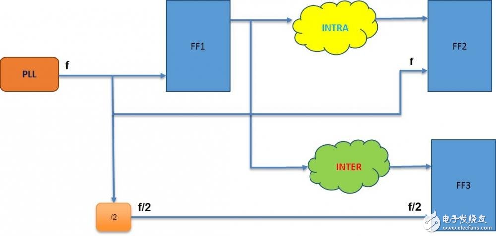
Figure 1: Internal clock domains and cross-clock domain paths may introduce faults in the form of delays.
A clock filter circuit (CFC) for transition fault testing filters out the required clock pulses from the clock source. Typical CFCs have limitations and cannot be used to test transition faults across cross-synchronous clock domains. What happens when a transition error occurs? We will explain these limitations and recommend improvements to the CFC to make the SCCD test (cross-clock domain failure as shown in Figure 1) feasible.
Figure 2 shows a typical clock filter circuit with three main components.
• The sync unit synchronizes the scan enable (SE) signal with the active clock domain.
• A programmable shift register triggered by a synchronous SE signal controls the integrated clock gating (ICG) to generate the required number of clock pulses.
• ICG unit.
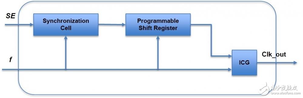
Figure 2: A typical clock filter circuit may not be sufficient to test for clock failures across the synchronous clock domain.
The full speed fault test consists of two steps. The first step is the shift mode and the second step is the capture mode. In shift mode, when SE is high, the register is initialized to a known value via scan chain shift. In capture mode, when SE is low, the response of the functional path is captured into the register.
In capture mode, the CFC is used to generate the required clock pulses for the start and capture cycles of the full speed test.
When the SE is strobed, it takes a delay to reach the CFC. Then in the CFC, it is synchronized with the two-stage synchronization unit of the receiving clock domain. The signal synchronized by the SE will trigger an n-level programmable register to provide an enable signal to the ICG to filter out the desired clock pulse. This means that the clock distance from the CFC has a certain delay from the moment the SE reaches the CFC. The delay is mainly caused by the synchronization unit delay.
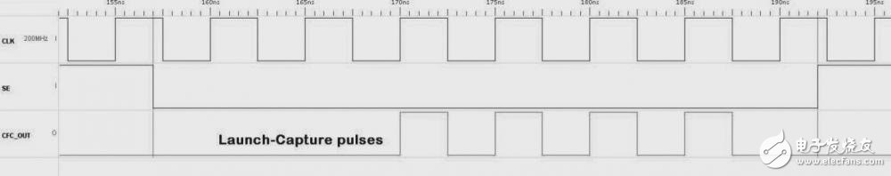
Figure 3: Typical CFC output waveform for a full speed test clock.
To test for failures in the clock domain (internal clock domain failures), the CFC is doing its part, as shown in Figure 3. However, to test the SCCD transition fault, a start and capture pulse needs to be generated, as shown in Figure 4. To get this waveform, we usually use two separate CFCs. Each clock domain requires its own CFC, because each clock has a different pulse width and therefore needs to be generated from a different CFC. Figure 4 shows an example of the different startup and capture conditions you can implement.
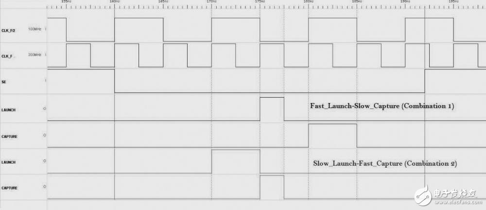
Figure 4: Typical start-up and capture pulse combinations for testing across clock domain faults, including fast start and slow capture as well as slow start and fast capture pulses.
When used to test for failures in the synchronous complex clock domain (Figure 1), the same CFC encountered the following challenges:
*** Edge missing ***: When testing for faults between two SCCDs, each clock domain has its own CFC. The output delay is caused by the inherent synchronization delay of the CFC. The resulting clock edges will not be period aligned. For example, assume two synchronous clocks of frequency F and F/2, each having a programmable CFC with a shift register length of four. Programmable shift registers are triggered at different times, resulting in different delays in the CFC output. Assuming a two-stage synchronizer, the clock domain F/2 requires twice the time of the clock domain F. Figure 5 shows the clock output waveforms of the two CFCs. It should be noted that there are two types of misalignment. One is due to the delay of the synchronization itself, as shown in Figure 5.
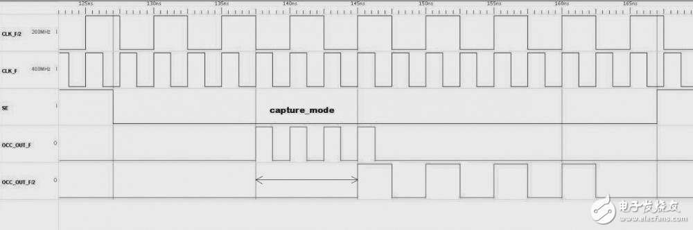
Figure 5: Clock waveform of the general-purpose CFC output showing the missing edge.
Another cause of misalignment is clock skew. The skew of each clock causes a further increase in the misalignment of the two CFC clock outputs. As shown in Figure 6, the output of CFC_OUT_F is skewed relative to CFC_OUT_F/2. Because of this, the functional timing window for capturing the transmitted signal is compressed, jeopardizing the quality and effectiveness of the test.
Warning Light,Revolving Light,Rotary Beacon
Chinasky Electronics Co., Ltd. , https://www.chinacctvproducts.com