First, LED history
50 years ago, people already knew the basics of light generated by semiconductor materials. In 1962, General Electric's Nick Holonyak Jr. developed the first practical application of visible light-emitting diodes. LED is the abbreviation of English light emitTIng diode. Its basic structure is an electroluminescent semiconductor material placed on a leaded shelf and then sealed with epoxy resin, that is, solid package, so it can To protect the internal core wire, the LED has good seismic performance.
The LED was originally used as an indicator light source for instrumentation. Later, various light-colored LEDs were widely used in traffic lights and large-area displays, resulting in good economic and social benefits. Taking a 12-inch red traffic light as an example, in the United States, a long-life, low-efficiency 140-watt incandescent lamp was used as a light source, which produced 2000 lumens of white light. After passing the red filter, the light loss is 90%, leaving only 200 lumens of red light. In the newly designed lamp, Lumileds used 18 red LED light sources, including circuit losses, to consume 14 watts of electricity, which would produce the same light effect. Automotive signal lights are also an important area for LED light source applications.
Second, the principle of LED chip
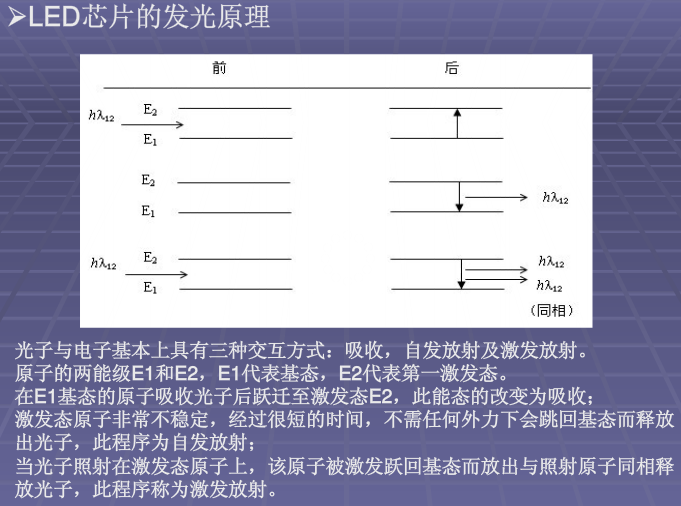
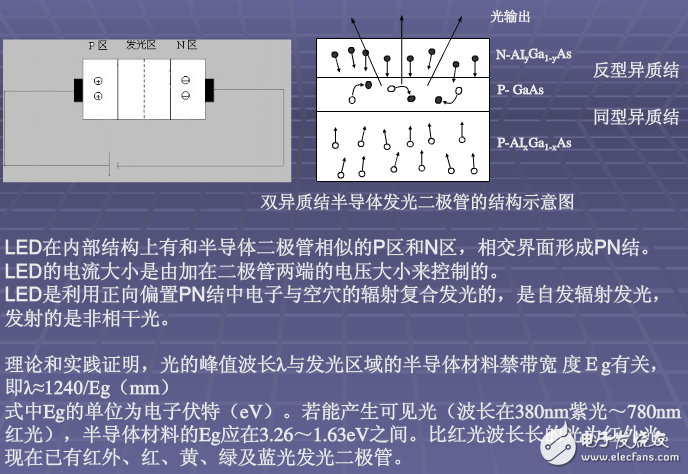
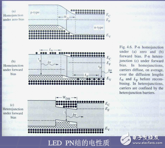
LED (Light EmitTIng Diode), a solid-state semiconductor device that converts electricity directly into light. The heart of the LED is a semiconductor wafer with one end attached to a holder, one end being the negative pole and the other end connected to the positive pole of the power supply, so that the entire wafer is encapsulated by epoxy. The semiconductor wafer consists of two parts, one part is a P-type semiconductor, in which the hole dominates, and the other end is an N-type semiconductor, which is mainly electrons here. But when the two semiconductors are connected, they form a "PN junction" between them. When a current is applied to the wafer through the wire, the electrons are pushed toward the P region. In the P region, the electrons recombine with the holes, and then the energy is emitted in the form of photons. This is the principle of LED illumination. The wavelength of light, which is the color of light, is determined by the material that forms the PN junction.

Third, the classification of LED chips
1.MB chip definition and characteristics
Definition: Metal Bonding chip; this chip belongs to the patented product of UEC.
Features:
(1) Using a material with a high heat dissipation coefficient, Si, as a substrate, heat dissipation is easy.
Thermal ConducTIvity
GaAs: 46W/mK
GaP: 77W/mK
Si: 125~150W/mK
Cupper: 300~400W/mk
SiC: 490W/mK
(2) Wafer bonding the epitaxial layer and the substrate through the metal layer while reflecting the photons to avoid absorption of the substrate.
(3) The conductive Si substrate replaces the GaAs substrate and has good thermal conductivity (the thermal conductivity is 3 to 4 times different), which is more suitable for the high driving current field.
(4) The bottom metal reflective layer is beneficial to the improvement of luminosity and heat dissipation.
(5) The size can be increased and applied to the High power field, eg: 42 mil MB.
2.GB chip definition and characteristics
Definition: Glue Bonding chip; this chip belongs to the patented product of UEC.
Features:
(1) A transparent sapphire substrate replaces a light-absorbing GaAs substrate, and its light output power is more than twice that of a conventional AS (Absorbable Structure) chip, and the sapphire substrate is similar to a GaP substrate of a TS chip.
(2) The chip emits light on all four sides and has an excellent Pattern.
(3) In terms of brightness, the overall brightness has exceeded the level of the TS chip (8.6 mil).
(4) Two-electrode structure, which is slightly inferior to the TS single-electrode chip in terms of high current resistance.
3.TS chip definition and characteristics
Definition: Transparent structure chip, which is a patented product of HP.
Features:
(1) The chip process is complex and much higher than the AS LED.
(2) Excellent reliability.
(3) A transparent GaP substrate that does not absorb light and has high brightness.
(4) Wide range of applications.
4.AS chip definition and characteristics
Definition: Absorbable structure chip; After nearly 40 years of development efforts, Taiwan's LED optoelectronics industry is at a mature stage in the research and development, production and sales of this type of chip, and the research and development level of major companies in this area is basically at At the same level, the gap is not big.
The mainland chip manufacturing industry started late, and its brightness and reliability still have a certain gap with the Taiwanese industry. Here we talk about the AS chip, especially the UEC AS chip, eg: 712SOL-VR, 709SOL-VR, 712SYM- VR, 709SYM-VR, etc.
Features:
(1) The quaternary chip is prepared by the MOVPE process, and the brightness is brighter than that of the conventional chip.
(2) Excellent reliability.
(3) Wide range of applications.
Fourth, LED chip material epitaxial type
1.LPE: Liquid Phase Epitaxy (liquid phase epitaxy) GaP/GaP
2.VPE: Vapor Phase Epitaxy GaAsP/GaAs
3.MOVPE: Metal Organic Vapor Phase Epitaxy (Organic Metal Vapor Phase Epitaxy) AlGaInP, GaN
4.SH: GaAlAs/GaAs Single Heterostructure (single-isotype structure) GaAlAs/GaAs
5.DH: GaAlAs/GaAs Double Heterostructure (Doubly Heterostructure) GaAlAs/GaAs
6.DDH: GaAlAs/GaAlAs Double Heterostructure (double heterostructure) GaAlAs/GaAlAs
Five, LED chip composition and lighting
The composition of the LED wafer: mainly composed of several elements such as arsenic (AS) aluminum (AL) gallium (Ga) indium (IN) phosphorus (P) nitrogen (N) bismuth (Si).
Classification of LED chips:
1. According to the brightness of the light:
A, general brightness: R, H, G, Y, E, etc.
B, high brightness: VG, VY, SR, etc.
C, super high brightness: UG, UY, UR, UYS, URF, UE, etc.
D, invisible light (infrared): R, SIR, VIR, HIR
E, infrared receiving tube: PT
F, photocell: PD
2, according to the composition of the elements:
A, binary wafer (phosphorus, gallium): H, G, etc.
B, ternary wafer (phosphorus, gallium, arsenic): SR, HR, UR, etc.
C, quaternary wafer (phosphorus, aluminum, gallium, indium): SRF, HRF, URF, VY, HY, UY, UYS, UE, HE, UG
3. LED chip characteristics table:
LED chip type illuminating color component element wavelength (nm)
SBI Blue lnGaN/sic 430 HY Ultra Bright Yellow AlGalnP 595
SBK brighter blue lnGaN/sic 468 SE highlight orange GaAsP/GaP 610
DBK brighter blue GaunN/Gan 470 HE super bright orange AlGalnP 620
SGL blue green lnGaN/sic 502 UE brightest orange AlGalnP 620
DGL brighter green LnGaN/GaN 505 URF brightest red AlGalnP 630
DGM brighter blue lnGaN 523 E orange GaAsP/GaP635
PG Pure Green GaP 555 R Red GAaAsP 655
SG standard green GaP 560 SR brighter red GaA/AS 660
G green GaP 565 HR super bright red GaAlAs 660
VG brighter green GaP 565 UR brightest red GaAlAs 660
UG brightest green AIGalnP 574 H high red GaP 697
Y yellow GaAsP/GaP585 HIR infrared GaAlAs 850
VY brighter yellow GaAsP/GaP 585 SIR infrared GaAlAs 880
UYS brightest yellow AlGalnP 587 VIR infrared GaAlAs 940
UY brightest yellow AlGalnP 595 IR infrared GaAs 940
Which is the most welcome kid laptop for entertainment and online learning? 10.1 inch laptop is the best choice. You can see netbook 10.1 inch with android os, 10.1 inch windows laptop, mini laptop 10.1 inch 2 in 1 windows, 10.1 inch 2 In 1 Laptop with android os. Of course, there are various matches of memory and storage, 2 32GB or 4 64GB. Our suggestion is that 10.1 inch android 32GB laptop, 10.1inch 32GB or 64GB Solid State Drive windows laptop. Except 10.1 inch Student Laptop , there are 11 Inch Laptop, 15.6 Inch Laptop, 14 Inch Laptop , also option here.
Besides, other advantages you can see on 10.1inch Budget Laptop For Students, for example, lightweight, competitive cost, portability, Android or Windows OS, rich slots, energy saving cpu, etc.
As a professional manufacturer, can provide free custom service, like mark client`s logo on laptop cover, opening system, inner color box, manual, boot. Produce as your special requirement on parameters, preinstall apps needed, etc. What you need to do is very simple, confirming PI, including price, delivery time, parameters, etc.
10.1 Inch Laptop,Netbook 10.1 Inch,10.1 Inch 2 In 1 Laptop,10.1 Inch Windows Laptop,Mini Laptop 10.1 Inch
Henan Shuyi Electronics Co., Ltd. , https://www.shuyipcs.com