In recent years, the market for portable electronic devices in the fields of mobile communication and mobile computing has been rapidly promoted, which has directly promoted the development of small-package and high-density assembly technologies. At the same time, it has also imposed a series of strict requirements on small package technologies, such as requiring package dimensions as much as possible. Shrinking (especially package height less than 1mm), the reliability of the connection after packaging is as high as possible, adapting to lead-free soldering (protecting the environment) and trying to reduce costs. Is the demand for device packaging in today's portable electronic devices so strict? In fact, maybe the third-generation cellular phone in your hand has used a very thin QFN package. The display panel on such a mobile phone is packaged in a power LSI and an intelligent power LSI circuit for driving a motor in a digital camera, and the requirements are strictly strict. Fortunately, these circuit devices use few lead wires, otherwise it is almost impossible to achieve
QFN packageQFN (Quad Flat No-lead Package, square flat leadless package), one of the surface mount packages. Now more called LCC. QFN is the name given by the Japan Electromechanical Industry Association. The four sides of the package are equipped with electrode contacts. Due to the absence of leads, the placement area is smaller than QFP and the height is lower than QFP. However, when stress is generated between the printed substrate and the package, no relief can be obtained at the electrode contact. Therefore, the electrode contacts are difficult to make as many pins as the QFP, generally from about 14 to about 100. The materials are ceramic and plastic. When there is an LCC mark, it is basically a ceramic QFN. The center of the electrode contacts is 1.27 mm. Plastic QFN is a low cost package of glass epoxy printed substrate. In addition to the 1.27mm center distance of the electrode contacts, there are two types of 0.65mm and 0.5mm. This package is also known as plastic LCC, PCLC, P-LCC, and the like.
Package structure selectionThere are many types of miniaturized package structures, such as ball grid array BGB packages, but the cost of the internal wiring substrate is much lower than that of QFP. However, the leads drawn from the current QFP structure are fan-shaped and fan-out, occupying a large assembly area (the assembly area in the mobile phone is very limited), which cannot meet the requirements. In 2000, JEDEC developed an improved specification called QFN (Quad Flat NonLeaded Package). As the name suggests, QFN folds the lead wire from the QFP fan back to the bottom of the package (becomes a strip contact line), which saves assembly area and further miniaturization.
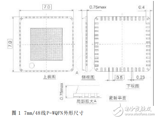
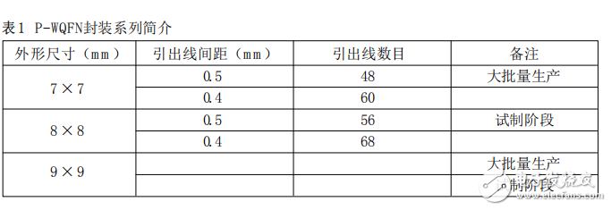
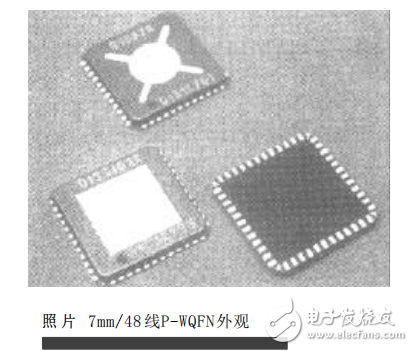
The technicians of NEC's Semiconductor Division developed a QFN structure of plastic (plasTIc) according to QFN standard specifications, which is very thin (very verythin=W), referred to as P-WQFN package structure. The projection of the package is shown in Figure 1. The appearance is shown in the photo. The P-WQFN package series is shown in Table 1.
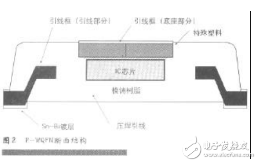
An overview of the manufacturing process can be seen from the cross-sectional structural view of the P-WQFN package shown in Fig. 2. It is a mold-casting resin that molds the soldered lead chips in a resin, and the circuit leads from the bottom. The bottom of the surface (pad) has a metal coating for reflow soldering. Since the lead-free soldering is required, the plating of the exposed portion of the lead wire is not a SnPb alloy but a Sn-Bi alloy.
First, the P-WQFN package exhibits good heat resistance during assembly. Because the high-temperature process that can withstand 260 ° C (highest) reflow is fully considered in the selection stage of raw materials and structures, the P-WQFN package can smoothly pass the reflow process at 260 ° C during reflow soldering (reflow soldering) The procedure stipulates that the 260 ° C high temperature processing time is no more than 10 seconds, and the 220 ° C high temperature processing time does not exceed 60 seconds). In particular, it should be pointed out that the reason why the P-WQFN package can exhibit good heat resistance is that the special high temperature resistant resin and the lead frame substrate for bonding between the selected IC chip and the lead frame are barely bonded in the design. Use on the surface of the plastic to prevent deformation from cracking (to prevent breakage and peeling due to thermal stress during high temperature reflow). In addition, the surface of the lead pad exposed on the bottom surface of the PWQFN has a SnBi plating layer, and the solder for reflow soldering (Sn-3Ag-0.5Cu) can be firmly soldered during reflow soldering.
Secondly, P-WQFN is packaged in the whole machine assembly (mobile phone, digital camera, etc.) and shows good reliability. To confirm this, a series of reliability tests can be performed prior to commercialization based on assembly applications such as cell phones and digital cameras. For example, the 9mm/64-line P-WQFN package will soon be commercialized and it has successfully passed reliability testing. The reliability test content includes many items, such as cycle, bending and pressurization; if a certain amount of samples are not damaged in the reliability test, the reliability test level can be passed. For example, drop test on five 9mm/64-line P-WQFN packages, free fall from 100cm height (including the X, Y, and Z faces of P-WQFN, respectively, landing twice, no damage found; other test results There is no damage. The 9mm/64-line P-WQFN package is commercialized, and the 7mm/48-line PWQFN has already been commercialized.
summaryThe P-WQFN package is a packaged product that targets the portable device market such as mobile phones and digital cameras. Because it meets the stringent requirements of this application, it will replace the old packaging such as QFP/SOP in this field. Especially suitable for lead-free soldering art, in line with environmental protection requirements.
T Copper Tube Terminals,Non-Insulated Pin-Shaped Naked Terminal,Copper Cable Lugs Terminals,Insulated Fork Cable Spade Terminal
Taixing Longyi Terminals Co.,Ltd. , https://www.txlyterminals.com