The 74LS373 is a commonly used address latch chip consisting of eight parallel D flip-flops with tri-state buffered outputs. In order to extend the external memory in a microcontroller system, a 74LS373 chip is usually required. This article will introduce the working principle of the 74LS373, covering the pin diagram, internal structure, main parameters and typical application circuits in the MCU expansion system.
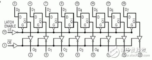
First, 74ls373 pin diagram and function introduction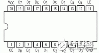
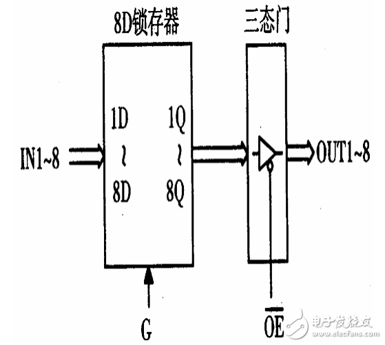
G is the data entry end: When G is "1", the latch output state (1Q ~ 8Q) is the same as the input state (1D ~ 8D); when G changes from "1" to "0", the data is locked In the memory.
(1).1 pin is output enable (OE), which is active low. When pin 1 is high, regardless of input 3, 4, 7, 8, 13, 14, 17, 18, no matter 11 How the pin (latch control terminal, G), output 2 (Q0), 5 (Q1), 6 (Q2), 9 (Q3), 12 (Q4), 15 (Q5), 16 (Q6), 19 (Q7 ) all exhibit a high-impedance state (or a floating state);
(2). When pin 1 is low, as long as a falling edge appears on pin 11 (latch control terminal, G), output 2 (Q0), 5 (Q1), 6 (Q2), 9 (Q3), 12 (Q4) 15, 15 (Q5), 16 (Q6), and 19 (Q7) immediately present the states of the input pins 3, 4, 7, 8, 13, 14, 17, and 18.
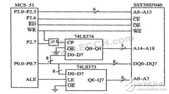
When the latch terminal LE goes from high to low, the 8-bit information at the output is latched until the LE terminal is valid again. When the tri-state gate enable signal OE is low, the tri-state gate is turned on, allowing Q0~Q7 output, and when OE is high, the output is left floating. When the 74LS373 is used as an address latch, OE should be made low. When the latch enable C is high, the output Q0~Q7 states are the same as the input terminals D1~D7; when C is negative During the transition, the input terminals D0~D7 are locked into Q0~Q7. The ALE signal of the 51 MCU can be directly connected to the C of the 74LS373. 74ls373 and microcontroller interface:
1D~8D is 8 inputs. 1Q~8Q is 8 outputs.
G is the data latch control terminal; when G=1, the latch output is the same as the input; when G changes from "1" to "0", the data is input into the latch.
OE is the output enable end; when OE=“0â€, the tri-state gate is open; when OE=“1â€, the tri-state gate is closed and the output is in a high-impedance state.
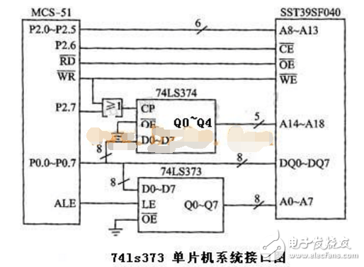
In the MCS-51 microcontroller system, the 74LS373 is often used as an address latch. The connection method is shown in the figure above. The input terminals 1D~8D are connected to the P0 port of the single chip microcomputer, the output terminal provides the low 8-bit address, and the G terminal is connected to the address latch enable signal ALE of the single chip microcomputer. The output enable terminal OE is grounded, indicating that the output tri-state gate is always open.
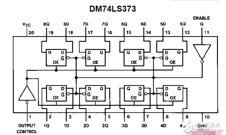
Third, 74ls373 logic circuit truth table1, 74LS373 logic diagram
2, 74ls373 truth table
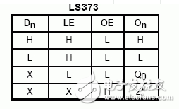
L--low level;
H--high level;
X--indeterminate state;
Q0--establish the level of Q before steady state;
G-- input terminal, connected with 8031ALE high level: unblocked low level: close the door latch. In the figure, OE--enable end, ground.
When G = "1", the 74LS373 output 1Q-8Q is the same as the input 1D-8D;
When G is the falling edge, the input data is latched.
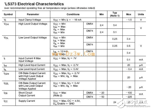
Fourth, 74ls373 parameters1, 74LS373 electrical parameters
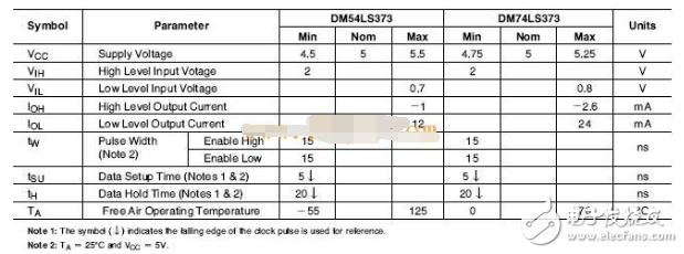
2, 74ls373 recommended working conditions
When 74LS373 is used as the address latch, OE should be made low. When latch enable G is high, the state of output Q0-Q7 is the same as that of input D1-D7; when G is negative During the transition, the input D0-D7 data is locked into Q0-Q7. The ALE signal of the 51 MCU can be directly connected to the G of the 74LS373. In the MCS-51 microcontroller system, the connection method is shown in the figure below. The input terminal 1D-8D is connected to the P0 port of the single chip microcomputer, the output terminal provides the low 8-bit address, and the G terminal is connected to the address latch enable signal ALE of the single chip microcomputer. The output enable terminal OE is grounded, indicating that the three-state output gate is always on, and the address signal can be sent.
The 1D-8D is 8 inputs. 1Q-8Q is 8 outputs.
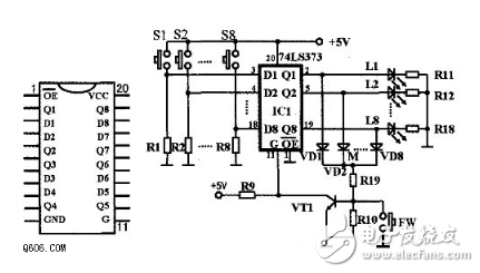
2, using the 74LS373 design of the answering device circuit diagramThe 74LS373 designed the responder circuit consists of an 8D latch 74LS373. 8 groups of key switches S1-S8, 8 groups of valid status display LEDs L1-L8, a reset button FW and so on.
The 8-way competition responder, each group is controlled by a rush button switch, and the high level indicates that the rush is valid.
The moderator control button FW is used to control the startup of the entire system and the effective start control of the rush. When the reset button FW is pressed, the control terminal G of the 8D latch is at a high level, and if any of the group button switches S1 to S8 is not pressed, that is, the input terminal D of the corresponding 8D latch is When it is low level, then the 8 output terminals are all low level, and the corresponding LEDs are not lit, indicating that the responder is preparing for the answering state. When the reset button FW is pressed, the control terminal G of the 8D latch is at a high level, and if one or several of the group button switches S1-S8 are in a pressed state, the input of the corresponding 8D latch is corresponding. The terminal D is at a high level, and the output end of the corresponding 8D latch is immediately at a high level, and the corresponding LED is lit, indicating that the responder is in violation. Only when the reset button FW is pressed once and the reset button FW is raised, the answer is valid.
The system has a first rush signal discrimination and latching function. After the host resets the system and the answer is valid, the first responder presses the answer button. The corresponding input pin is connected to the high potential 1. The corresponding output of the 8D latch is immediately high 1. Diodes VD1-VD8 form an OR gate circuit. The base of the transistor VT1 is brought to a high potential and saturating is turned on to make the G of the latch low, and the input signal of the 8D latch is latched at the output, and the signal change at the input will not affect the output. The corresponding illuminated LED indicates the group of the first responder.
Buzzer alerts can also be used at the same time as valid groups are displayed.
Device selection and circuit fabrication
The 8D latch selects the 74LS373, and its pinout diagram is shown in Figure 2. If you choose another model, pay attention to the requirements of the control level and other enable terminals. 8 group button switches S1-S8 and reset button FW can be used to select the AN8 series lathe control buttons. 8 groups of valid status display LEDs L1 ~ L8 select φ10 high-brightness LED; triode VT1 select S9014, resistor R1-R8 select 025W / 5.1kΩ, R11 ~ R18 select ~ 25W / 430Ω, R9 and R10 selection 0.25W/5.1kΩ, R19 selects 0.25W, 5,10Ω, and diodes VDl~VD8 select IN4148.
The circuit is powered by a single 5V supply and can be obtained with a 7805 voltage regulator integrated circuit.
During production, the answer button and indicator LED can be taken out from the circuit board through the terminal block, which is convenient for use.
Assembly and welding are correct, which guarantees reliable operation.
Design Features
The control signal of the enable terminal G of the 8D latch 74LS373 is not a periodically fixed pulse signal, but is obtained by processing the signal taken from the output of the latch, ensuring the most compact circuit structure, the fastest processing time, and reducing the pulse. The source may have interference that makes the circuit performance more reliable.
Insulated Copper Tube Terminals
Insulated Copper Tube Terminals,High quality insulated terminal,copper tube terminal
Taixing Longyi Terminals Co.,Ltd. , https://www.longyiterminals.com