The clock is a reference for all signals in a digital circuit, especially in an FPGA. The clock is the power of the sequential circuit, the blood, and the core. If there is no clock or the clock signal is not processed properly, it will affect the performance and even the function of the system. Therefore, in general, the same clock source is used in the same design. When there are multiple clocks in the system, you need to choose different according to different situations. The processing method is to synchronize all the clocks. The following describes the synchronization processing method of the clock in several cases.

The first case:
When there are multiple clocks in the same digital circuit, and one clock (Clk) is more than twice as fast as the other clocks.
This situation is the simplest. In the interface part, other clocks must be synchronized and processed into a clock signal synchronized with Clk.
The benefits of this treatment are:
Easy to handle internal timing of the circuit;
The inter-clock boundary conditions are only processed in the interface part circuit.
In essence, the synchronous processing method of clock sampling is the rising edge extraction circuit, and the output information is extracted through the rising edge, and the information of the system clock is provided, so that the reliability and portability of the circuit are ensured.
The second case:
When all clocks in the system do not have a clock rate that is twice the frequency of other clocks, that is, multiple clock rates in the system are similar.
At this time, the sampling theorem cannot be satisfied, so in the interface part, other clocks and data must be isolated by FIFO or DPRAM, and other clock information is converted into an allowable signal synchronized with the system clock. For example, in a high-speed data acquisition system, the acquisition clock of AD tends to be relatively high, more than half of the system clock. At this time, synchronization processing cannot meet the timing design.
The third case:
Data is sampled between multiple clocks in the system.
In this case, two levels of flip-flops can be used to cascade the sampled data to avoid metastability.
The fourth situation:
Multi-level clock network processing.
The so-called multi-level clock network refers to the clock input terminal connected to the flip-flop after the clock passes more than one level of the gate circuit.
Due to the clock setup-hold time limitation, multi-clock networks should be avoided in FPGA design. In the design, the clock network must be simplified, and the enabled mode or other simplified circuit structure should be used as much as possible.
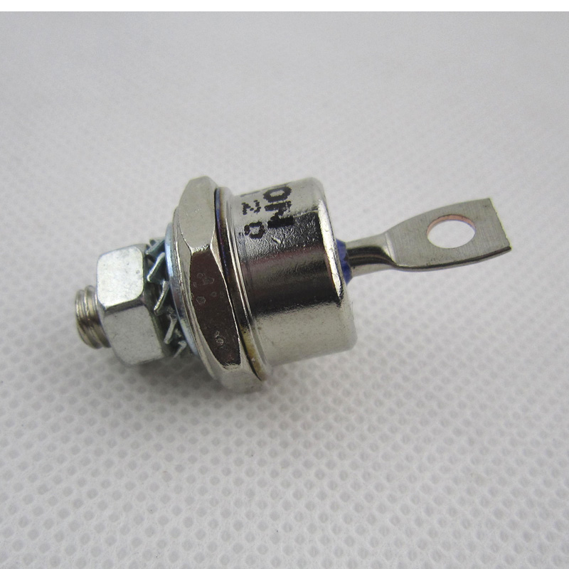
Fast Recovery Diode (FRD) is a semiconductor diode with good switching characteristics and short reverse recovery time. It is mainly used in switching power supplies, PWM pulse width modulators, inverters and other electronic circuits as high-frequency rectifier diodes. Free-wheeling or damper diodes are used. The internal structure of the fast recovery diode is different from that of an ordinary PN junction diode. It belongs to a PIN junction diode, that is, a base region I is added between the P-type silicon material and the N-type silicon material to form a PIN silicon wafer. Since the base area is thin and the reverse recovery charge is small, the fast recovery diode has a short reverse recovery time, a low forward voltage drop, and a high reverse breakdown voltage (withstanding voltage).

Fast Recovery Stud Diode,Stud Type Fast Recovery Diode,Fast Recovery Diode,Stud Rectifier Power Diode
YANGZHOU POSITIONING TECH CO., LTD. , https://www.cndingweitech.com