The output current of the photoelectric sensor is a key performance parameter of the photoelectric sensor. The output current of the photoelectric sensor is not only related to the design of the transmitter radiation intensity and the receiver collector current, the distance or angle between the transmitter and the receiver, the size of the transmitter and the front slot of the receiver, but also the components. It is related to the manufacturing process control of the outer casing, the process control of the assembly process, and the testing process. On the basis of analyzing the factors affecting the output current of photoelectric sensor in the design and manufacturing process, it is proposed to improve the radiation intensity and collector current of the transmitter and receiver, strengthen the process control of production and manufacturing process, and classify the products to improve the product. Rate of measures.
Photoelectric sensors are widely used in production process automation, office automation equipment, medical equipment, light control toys and other industries, and are constantly being applied in some new research fields, such as intelligent vehicle automatic tracing system, clinical medical testing, automatic seam tracking. Systems, military equipment, energy utilization systems, etc. Commonly used photoelectric sensors include a Transmissive OpTIcal Sensor and a Reflective Optoelectronic Sensor (ReflecTIve OpTIcal Sensor). Both the slot type and the reflective type photosensor are assembled by a light emitting device, that is, an emitter (Emitter) and a light receiving device, that is, a Detector. The slot type photoelectric sensor mounts the transmitter and the receiver at a distance from the housing, and the infrared or visible light emitted by the transmitter reaches the receiver through the slot of the housing to detect whether there is any object blocking between the transmitter and the receiver. The reflective photosensor mounts the transmitter and receiver at an angle to the housing to detect the presence of reflective or reflective media in front of the sensor. The basic characteristics of the photoelectric sensor include the relationship between the output current and the voltage across the receiver, the relationship between the output current and the input current of the transmitter, the relationship between the output current and the temperature, and the impulse response characteristic curve. Although the slot type and reflective photoelectric sensors are not complicated from the working principle, it is not easy to design and manufacture a photoelectric sensor that meets the requirements, stable performance, good reliability and reasonable cost, not to mention some applications. Sensor performance parameters are very demanding. This paper discusses the factors affecting the output current of photoelectric sensors from the perspective of design and manufacturing, and proposes some corresponding measures to improve the yield of the sensor manufacturing process.
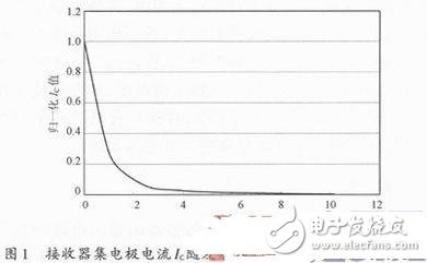
1 transmitter and receiver selectionThe output current ICON of the photosensor is a very critical parameter of the photosensor. For slot-type photosensors, ICON is not only related to transmitter radiant Ee, receiver collector current IC, but also transmitter-receiver distance and transmitter-receiver front slot under given conditions. Width related. Figure 1 is a graph showing the receiver collector current IC as a function of distance measured at a transmitter current of 10 mA when the distance between the side-emitting emitter and the side-receiving receiver is changed. The larger the distance, the smaller the receiver collector current IC under the same conditions. The greater the width of the slot in front of the transmitter and receiver, the greater the output current ICON of the photosensor under the same conditions. In the design of the slot type photoelectric sensor, the emitter radiation intensity and the collector collector current should be combined with the distance between the emitter and the receiver, as well as the slot width.
For reflective photoelectric sensors, under certain conditions, ICON is not only related to the emitter radiation intensity Ee, the receiver collector current IC, but also the distance between the sensor and the reflective surface and between the transmitter and the receiver. Angle related. In the design process of the reflective photoelectric sensor, the emitter radiation intensity and the collector collector current should be selected in combination with the distance between the sensor and the reflecting surface and the angle between the emitter and the receiver.
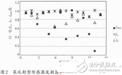
2 Process and manufacturing process impactIn general, a high-emitter radiant intensity Ee and a high-collector collector current IC are assembled with a photo-electric sensor whose output current ICON is also high, and vice versa. However, due to the deterioration in the process, testing and manufacturing process, there are many exceptions. Sample 6 and Sample 10 in Figure 2, although the emitter radiation intensity Ee of both is close, the receiver collector current IC of sample 10 is higher than the IC of sample 6, but the output current ICON of sample 10 is lower than that of sample 6. ICON; the emitter radiance Ee of sample 8 and sample 13 are similar to the receiver collector current IC, but the output current ICON of sample 8 is much higher; likewise, the emitter radiance Ee and reception of sample 1 and sample 5 The collector current ICs are similar, but the output current ICON of sample 5 is much lower. There are many factors influencing this situation, including the dimensional deterioration caused by the plastic casing injection molding process, the variation caused by the sensor assembly process, the spatial variation of the emitter radiation intensity, and the error caused during the test.
(1) The outer casing size is deteriorated. Most of the housings of the slot and reflective photoelectric sensors are made of plastic housing. Mold processing, injection molding and cooling of the injection molded parts will cause changes in the same size between different plastic housings. This includes slot type photoelectric sensor transmitters and receivers. Variation of the slot width in front of the device, changes in the distance between the transmitter and the receiver portion on the housing, changes in the size of the front aperture of the reflective photosensor transmitter and receiver, and mounting of the transmitter and receiver on the housing Changes in angle between parts, etc. These changes in size will cause a change in the sensor output current.
(2) Variations that occur during the assembly process. The assembly and fixing of the transmitter, receiver and housing in the slot type and reflective photoelectric sensor needs to be completed by a certain process, such as a slot type photoelectric sensor, and the housing and receiver can be heat-pressed for some housing materials. Fixed to the outer casing. In the assembly process, for the slot photoelectric sensor, the optical axis of the transmitter lens is not guaranteed to be on the same line as the optical axis of the receiver lens. Some products deviate from the design requirements, while others deviate from the larger; For reflective photoelectric sensors, the intersection of the optical axis of the emitter lens and the optical axis of the receiver lens is not likely to be exactly on the surface of the reflector as required by the design. Some products have intersections, while others may be backwards. some. Variations in these assembly processes can also cause changes in the sensor output current.
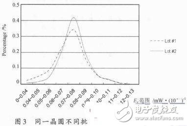
(3) Changes in the radiation intensity of the emitter and its spatial distribution The position of the wafer has an effect on the radiation intensity of the emitter and its spatial distribution. Under design conditions, the wafer is on the centerline of the emitter lens. However, in the manufacturing process of the transmitter, both the die-attach and the encapsulated process may cause the wafer to deviate from the centerline, and the deviation caused by the sealing process is generally larger. Figure 3 shows the distribution of the radiation intensity of different emitters of the same wafer. As can be seen from the figure, the ratio of the emitter of the batch 1 in the range of 0.07 to 0.08 mW/10° is 34.2%, and the ratio of the intensity of the batch 2 in the same range is 41.8%. Since the test of the radiation intensity of the emitter is generally different from the conditions of use of the emitter in the photosensor, the change in the spatial distribution of the radiation intensity may result in the photoelectric sensor of the high radiation intensity emitter obtained under the same conditions. The output current is lower than the photoelectric sensor of the low-radiation emitter obtained by the assembly test. In addition, in general, the refractive index of the silica gel used to fill the reflective cup and the cover wafer is very close to the refractive index of the epoxy resin used for sealing, so the shape of the interface between the silica gel and the epoxy resin is irradiated to the emitter. The effect of the intensity distribution is small. However, if there is a certain difference between the two, the shape of the interface will affect the radiation intensity distribution of the emitter. In this case, it is important to control the amount of silica gel used in the dispensing process to be the same or similar, so that different emitters of silica gel and The shape of the epoxy interface remains the same, avoiding variations in the spatial distribution of the emitter radiation intensity.
Remoter Controller,Remote Control,Wireless Remote, Universal Remote Control,universal remote
NINGBO COWELL ELECTRONICS & TECHNOLOGY CO., LTD , https://www.cowellsocket.com